Flexible array substrate as well as manufacturing method and flexible display thereof

A flexible substrate and flexible array technology, which is applied in the manufacture of electric solid-state devices, semiconductor devices, semiconductor/solid-state devices, etc., can solve the problems of unfavorable narrow border effects, disconnection, and padending design structures that need to be improved.

Active Publication Date: 2017-09-01
BOE TECH GRP CO LTD
View PDF5 Cites 41 Cited by
  • Summary
  • Abstract
  • Description
  • Claims
  • Application Information

AI Technical Summary

Problems solved by technology

In the actual production process, due to the fluidity of the adhesive material, the thickness of B and C will generally be much lower than the middle position A, so it is easy to cause line breakage at positions D and E during bending
Therefore, in order to ensure a uniform glue thickness at the bending position, the glue material...

Method used


Image

  • Flexible array substrate as well as manufacturing method and flexible display thereof
  • Flexible array substrate as well as manufacturing method and flexible display thereof
  • Flexible array substrate as well as manufacturing method and flexible display thereof

Examples


Embodiment Construction

[0058] The following describes the embodiments of the present invention in detail, and those skilled in the art will understand that the following embodiments are intended to explain the present invention, and should not be regarded as limiting the present invention. Unless otherwise specified, in the following examples that do not explicitly describe specific techniques or conditions, those skilled in the art can carry out according to commonly used techniques or conditions in this field or according to product instructions. The reagents or instruments used were not indicated by the manufacturer, and they were all commercially available conventional products.

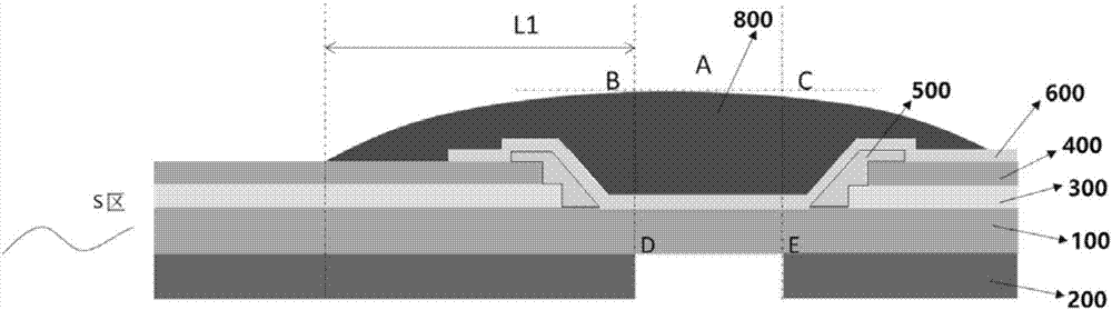
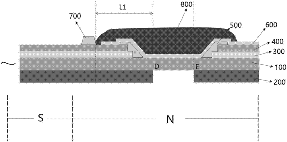
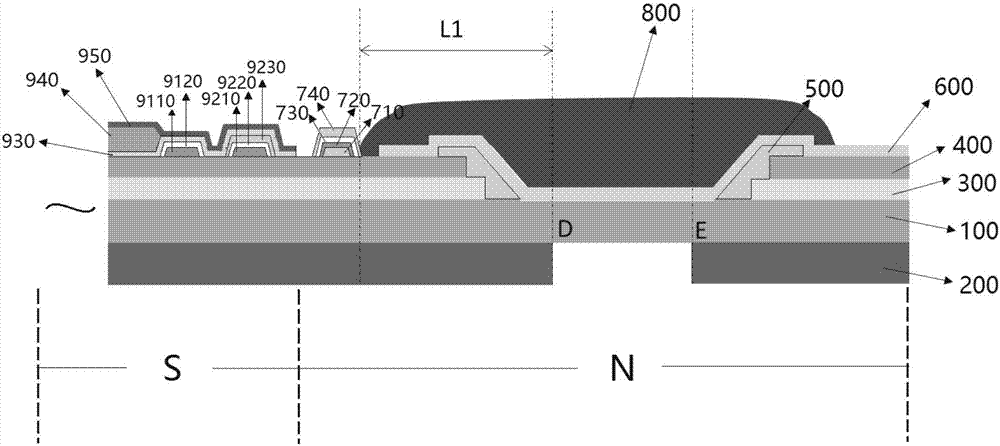
[0059] In one aspect of the present invention, the present invention provides a flexible array substrate. refer to Figure 2-4 , to describe the flexible array substrate of the present invention in detail.

[0060] According to an embodiment of the present invention, refer to figure 2 , the flexible array substrate...


PUM

PropertyMeasurementUnit
Heightaaaaaaaaaa
Widthaaaaaaaaaa

Abstract

The invention discloses a flexible array substrate as well as a manufacturing method and a flexible display thereof. The flexible array substrate comprises a flexible substrate, a display region arranged on one side of the flexible substrate, a non-display region arranged at the periphery of the display region, a protective layer used for covering a source and drain electrode layer of the non-display region and a protective layer block wall arranged on one side, close to the display region, of the non-display region and used for limiting a width of the protective layer. According to the flexible array substrate provided by the invention, the protective layer block wall is arranged on one side, close to the display region, of the non-display region and can limit a glue material from flowing toward a light emitting region when the protective layer of a bending region is manufactured, so that the width of the protective layer can also be limited while the uniformity of the coating thickness of the protective layer is guaranteed, a climbing region can be effectively shortened, and realization of the narrow frame effect is facilitated.

Description

technical field [0001] The invention relates to the technical field of flexible display screens, in particular, the invention relates to a flexible array substrate, a manufacturing method thereof, and a flexible display. Background technique [0002] At present, existing display products (such as Samsung Galaxy Note7) use the bendability of flexible substrates to bend the position (Fanout, fan-out area) where the pixel leads are connected to external circuits to achieve the effect of narrow borders, which we call Pad bending (Pad bending) design, the specific structure before bending can refer to figure 1 . Compared with rigid OLED, the Fanout area designed by pad bending does not use gate (Gate) leads, but uses source-drain electrode (SD) layer to connect with external circuits. On the SD surface, there are only organic layers such as organic film (PLN) and pixel definition (PDL), which are easily corroded by water vapor after bending. Therefore, protective glue should b...

Claims


Application Information

Patent Timeline
IPC IPC(8): H01L27/32H01L51/52H01L51/56
CPCH10K59/122H10K77/111H10K50/844H10K71/00
Inventor 付文悦许晨孙韬陈立强
Owner BOE TECH GRP CO LTD
Why Eureka
Try Eureka