

Array substrate, organic electroluminescence display panel and inkjet printing method
An array substrate and inkjet printing technology, which is applied to circuits, electrical components, and electrical solid-state devices, etc., can solve problems such as position shift and display color cross-talk, and achieve the effect of simple implementation process and solving display color cross-talk.
- Summary
- Abstract
- Description
- Claims
- Application Information
AI Technical Summary
Problems solved by technology
Method used
Image

Examples
Embodiment Construction
[0026] In order to make the purpose, technical solutions and advantages of the present invention clearer, the present invention will be further described in detail below in conjunction with the accompanying drawings. Obviously, the described embodiments are only some of the embodiments of the present invention, rather than all of them. Based on the embodiments of the present invention, all other embodiments obtained by persons of ordinary skill in the art without making creative efforts belong to the protection scope of the present invention.
[0027] The shapes and sizes of the components in the drawings do not reflect the real scale, but are only intended to schematically illustrate the content of the present invention.
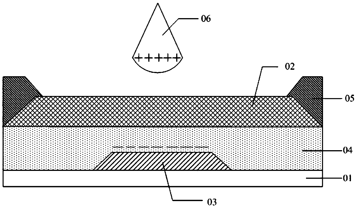
[0028] An array substrate provided by an embodiment of the present invention, such as figure 1 as shown, figure 1 A schematic cross-sectional structure diagram of an array substrate provided in an embodiment of the present invention; including a base subst...
PUM
 Abstract
Description
Claims
Application Information