Array substrate, electroluminescence display panel and display device

A technology of array substrate and substrate substrate, which is applied to circuits, electrical components, electrical solid devices, etc., to avoid color shift, improve brightness, and improve the utilization rate of light

Active Publication Date: 2018-07-13
WUHAN TIANMA MICRO ELECTRONICS CO LTD
View PDF11 Cites 18 Cited by
  • Summary
  • Abstract
  • Description
  • Claims
  • Application Information

AI Technical Summary

Problems solved by technology

[0004] Embodiments of the present invention provide an array substrate, an electroluminescence display panel, and a display device to solve the problems existing in the prior art of how to improve the display resolution of OLED displays and improve the quality of display images

Method used


Image

  • Array substrate, electroluminescence display panel and display device
  • Array substrate, electroluminescence display panel and display device
  • Array substrate, electroluminescence display panel and display device

Examples


Embodiment Construction

[0023] The specific implementation manners of an array substrate, an electroluminescence display panel, and a display device provided by embodiments of the present invention will be described in detail below with reference to the accompanying drawings. It should be noted that the described embodiments are only some of the embodiments of the present invention, but not all of the embodiments. Based on the embodiments of the present invention, all other embodiments obtained by persons of ordinary skill in the art without making creative efforts belong to the protection scope of the present invention.

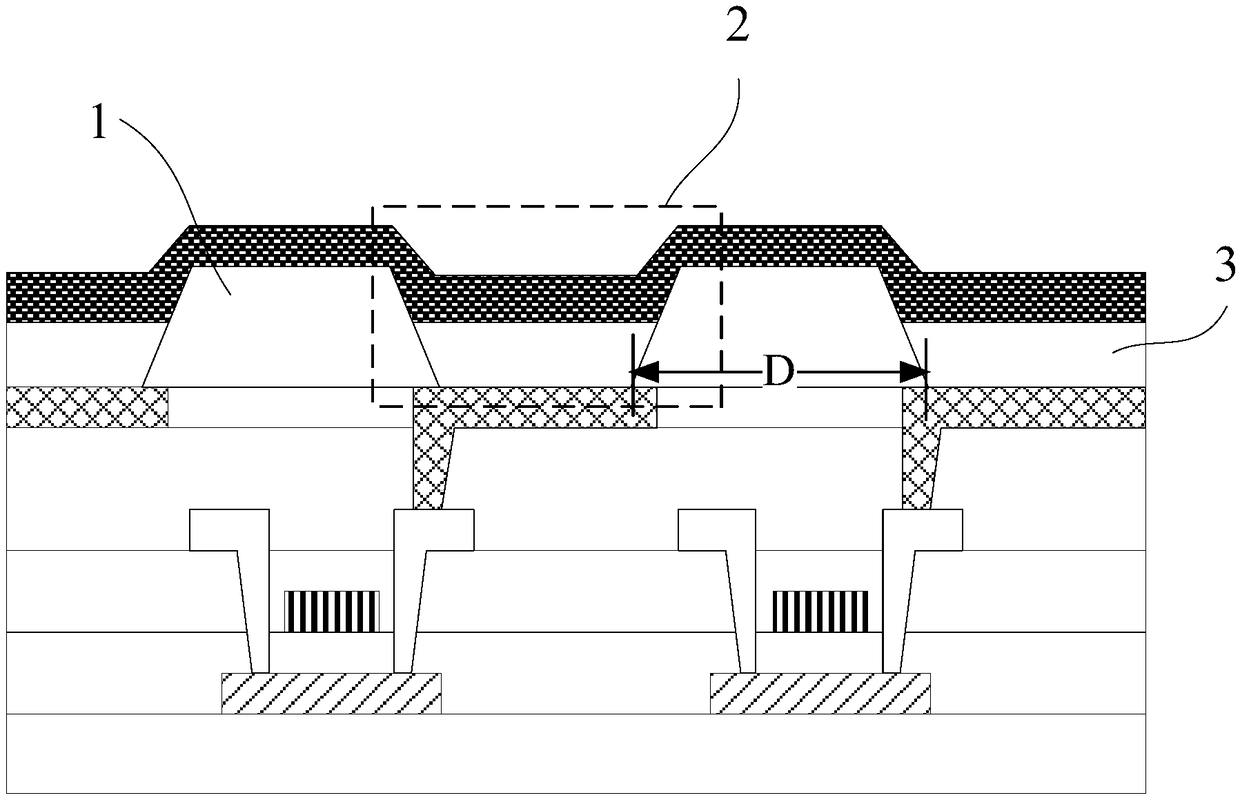
[0024] The inventor found in the research that in the structure of the existing OLED display, such as figure 1 As shown, a pixel defining structure 1 is usually provided, and a plurality of pixel regions 2 are defined by the pixel defining structure 1 (as shown in a dashed box 2), and a light emitting unit 3 is arranged in each pixel region 2 to realize a display display function....


PUM


Abstract

The invention discloses an array substrate, an electroluminescence display panel and a display device. With arrangement of an optical regulating structure, interference of light emitted from two adjacent pixel areas can be avoided effectively, a pixel limit structure can be quite thin, and thus area occupation of the pixel limit structure is reduced, while pixel density is increased correspondingly and display resolution ratio is improved. Besides, as the optical regulating structure has reflecting and scattering functions, the brightness of a display can be increased while the light utilization rate is increased, and accordingly image display quality can be improved effectively.

Description

technical field [0001] The invention relates to the field of display technology, in particular to an array substrate, an electroluminescence display panel and a display device. Background technique [0002] Among the existing displays, organic electroluminescent display (Organic Electroluminescent Display, OLED), as an active light-emitting display, has gradually become the mainstream in the display field due to its low power consumption, high color saturation, wide viewing angle and other characteristics. Moreover, with the development of display technology, people's requirements for displays are gradually increasing, especially in terms of display resolution. It is hoped that the display can have a higher display resolution to provide users with more refined and softer images. screen to improve user experience. [0003] Based on this, how to improve the display resolution of the OLED display and improve the quality of the displayed picture is a technical problem to be sol...

Claims


Application Information

Patent Timeline
Patent Type & Authority Applications(China)
IPC IPC(8): H01L27/32
CPCH10K59/121H10K59/13H10K59/12
Inventor 王湘成牛晶华
Owner WUHAN TIANMA MICRO ELECTRONICS CO LTD
Why Eureka
Try Eureka