Optical image recognition chip, manufacturing method and terminal device

An optical image and chip technology, which is used in printing image acquisition, character and pattern recognition, radiation control devices, etc., can solve problems such as low reliability and cumbersome process, and achieve the effect of reducing device cost.

Active Publication Date: 2022-07-15
SHENZHEN GOODIX TECH CO LTD
View PDF5 Cites 0 Cited by
  • Summary
  • Abstract
  • Description
  • Claims
  • Application Information

AI Technical Summary

Problems solved by technology

[0005] The invention provides an optical image recognition chip, a manufacturing method and a terminal device, which are used to solve the problems of low reliability and cumbersome process of the existing optical image recognition chip caused by lamination

Method used


Image

  • Optical image recognition chip, manufacturing method and terminal device
  • Optical image recognition chip, manufacturing method and terminal device
  • Optical image recognition chip, manufacturing method and terminal device

Examples


Embodiment Construction

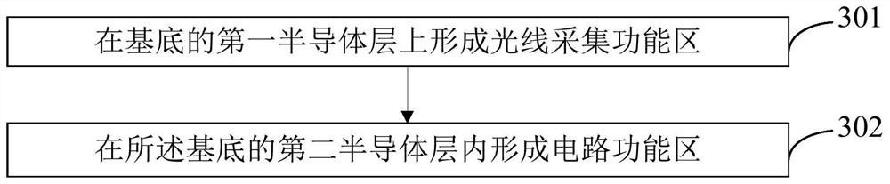
[0020] In order to make the purposes, technical solutions and advantages of the embodiments of the present invention clearer, the technical solutions in the embodiments of the present invention will be clearly and completely described below with reference to the accompanying drawings in the embodiments of the present invention. Obviously, the described embodiments These are some embodiments of the present invention, but not all embodiments. Based on the embodiments of the present invention, all other embodiments obtained by those of ordinary skill in the art without creative efforts shall fall within the protection scope of the present invention.

[0021] For the convenience of description, the sizes of different layers and regions are enlarged or reduced, so the sizes and ratios shown in the figures do not necessarily represent actual sizes, nor do they reflect the proportional relationship of sizes.

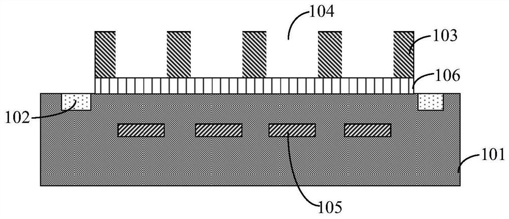
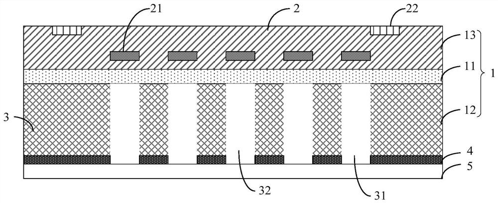
[0022] figure 2 A schematic structural diagram of the optical image reco...


PUM

PropertyMeasurementUnit
thicknessaaaaaaaaaa

Abstract

The invention provides an optical image recognition chip, a manufacturing method and a terminal device. The chip includes: a substrate, a circuit functional area and a light collection functional area; wherein, the substrate includes an insulating layer and a first semiconductor layer grown on a first surface of the insulating layer. , a second semiconductor layer grown on the second surface of the insulating layer; the light collection functional area is formed on the first semiconductor layer; the circuit functional area is formed in the second semiconductor layer; The optical signal is transmitted to the circuit functional area; the circuit functional area is used for image recognition according to the optical signal. The present invention realizes the further improvement of the integration degree of the product and the reduction of the process steps, thereby reducing the cost of the device. At the same time, it can avoid the influence of the tolerance caused by lamination and the shrinkage rate of the adhesive material on the reliability of the product.

Description

technical field [0001] The invention relates to chip technology, in particular to an optical image recognition chip, a manufacturing method and a terminal device. Background technique [0002] In existing terminal devices, optical image recognition chips are often used to complete functions such as fingerprint recognition. The optical image recognition chip mainly includes two parts: a circuit functional area for image recognition and a light collection functional area for transmitting light to the circuit functional area. Specifically, the light enters the circuit functional area through the light acquisition functional area for image recognition. [0003] figure 1 is a schematic structural diagram of an existing optical image recognition chip, such as figure 1 As shown, the chip mainly includes: an image recognition device 101 , a light collection channel cover plate 103 and an adhesive layer 106 . Wherein, the light collection channel cover 103 is attached to the surf...

Claims


Application Information

Patent Timeline
Patent Type & Authority Patents(China)
IPC IPC(8): H01L27/146G06V40/13
CPCH01L27/14625H01L27/1464H01L27/14683H01L27/14685G06V40/1318H01L27/146G06V10/10G06F18/00
Inventor 吴宝全沈健龙卫
Owner SHENZHEN GOODIX TECH CO LTD
Why Eureka
Try Eureka