Eureka AIR delivers breakthrough ideas for toughest innovation challenges, trusted by R&D personnel around the world.

Bulk material packaging equipment in semiconductor industry

A packaging equipment and semiconductor technology, applied in packaging, transportation packaging, packaging protection and other directions, can solve the problems of simplicity, bulk packaging equipment does not have a structure, etc., to improve convenience and safety, simplify operation, and solve the effect of simple structure

Inactive Publication Date: 2018-10-09
SUZHOU BOJI OPTOELECTRONICS TECH CO LTD
View PDF4 Cites 1 Cited by
  • Summary
  • Abstract
  • Description
  • Claims
  • Application Information

AI Technical Summary

Problems solved by technology

[0003] The invention provides a semiconductor industry bulk packaging equipment to solve the problem that the semiconductor industry bulk packaging equipment does not have simple structure, versatility and stability in the prior art

Method used


Image

  • Bulk material packaging equipment in semiconductor industry
  • Bulk material packaging equipment in semiconductor industry
  • Bulk material packaging equipment in semiconductor industry

Examples


Embodiment Construction

[0033] In order to make the technical means, creative features, objectives and effects of the invention easy to understand, the present invention will be further described below in conjunction with the accompanying drawings.

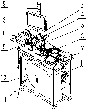
[0034] A kind of semiconductor industry bulk packaging equipment of the present invention, such as figure 1 As shown, a bulk material packaging equipment for the semiconductor industry, the bulk material packaging equipment includes a main body 1, the upper part of the main body 1 is provided with a workbench, the lower part of the main body 1 is provided with a locker, and the locker is provided with two storage doors that can be opened and closed. The object door is provided with rolling pulleys on the four corners of the main body 1 bottom.

[0035] The working table is equipped with a feeding system 2, a visual inspection system 3, an automatic pick-and-place system 4, a packaging system 5, a take-up system 6, a control system 7, and an electric cont...


PUM


Abstract

The invention relates to the field of packaging machinery or semiconductors, and discloses bulk material packaging equipment in the semiconductor industry. The packaging equipment comprises a main body, wherein the main body is provided with a band supply system, a feeding system, a visual detection system, an automatic material taking and placing system, a packaging system, a band receiving system and a control system, and the band supply system, the feeding system, the visual detection system, the automatic material taking and placing system, the packaging system and the band receiving system are used for completing the bulk material packaging operation under the control of the control system. According to the bulk material packaging equipment, the visual detection system and the automatic material taking and placing system are arranged, so that the universality for various products is achieved, and the production stability is improved; the purpose of simplifying the operation is achieved through centralized control of the control system; and therefore, the problem that bulk material packaging equipment in the semiconductor industry in the prior art does not has a simple structure, the universality and the stability is solved.

Description

technical field [0001] The invention relates to the field of packaging machinery or semiconductors, in particular to bulk packaging equipment in the semiconductor industry. Background technique [0002] With the rapid development of the semiconductor industry, the development of high-performance and high-efficiency packaging equipment is increasingly needed. Among them, the bulk packaging equipment is an important equipment on the semiconductor packaging production line except for the tray loading packaging machine and the tube loading packaging machine. Its performance and efficiency have a direct impact on production line throughput. The existing bulk packaging equipment in the semiconductor industry is either not universal, or has complex structure and operation, or poor stability, or low efficiency. It cannot meet the needs of modern production lines for production cost control and capacity control. To simplify the structure of bulk packaging equipment in the semico...

Claims


Application Information

Patent Timeline
Patent Type & Authority Applications(China)
IPC IPC(8): B65B35/34B65B35/38B65B51/14B65B9/02B65B57/00
CPCB65B9/02B65B35/34B65B35/38B65B51/14B65B57/00
Inventor 陈恕华胡晨光
Owner SUZHOU BOJI OPTOELECTRONICS TECH CO LTD
Why Eureka
Eureka Blog
Learn More