

Thimble anti-collision structure and ejector module
A thimble and anti-collision technology, which is applied in the manufacturing of electrical components, circuits, semiconductor/solid-state devices, etc., can solve the problems that the thimble module is easily hit and damaged.
- Summary
- Abstract
- Description
- Claims
- Application Information
AI Technical Summary
Problems solved by technology
Method used
Image

Examples
Embodiment Construction
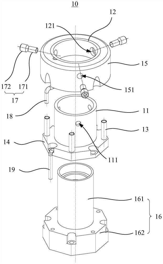
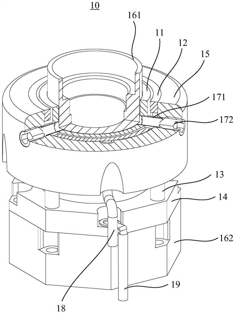
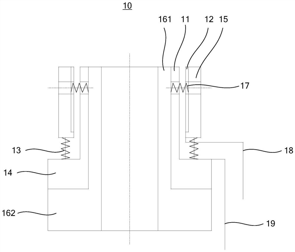
[0021] Such as Figure 1 to Figure 3 As mentioned above, in one embodiment, a thimble anti-collision structure 10 is provided, including a conductive cylinder 11 capable of inserting a thimble and a conductive ring 12 sleeved on the periphery of the conductive cylinder 11, and the outer periphery of the conductive cylinder 11 is provided with elastic A support member 13, one end of the elastic support member 13 is connected to the conductive cylinder 11, and the other end of the elastic support member 13 is connected to the conductive ring 12. When working normally, the conductive cylinder 11 is connected to the conductive cylinder 11. The conductive rings 12 are arranged at intervals, and the two are in a power-off state. When an external object hits, the conductive ring 12 moves relative to the conductive cylinder 11 , and the conductive ring 12 is in contact with the conductive cylinder 11 to be energized.
[0022] The above solution provides a thimble anti-collision struct...
PUM
 Abstract
Description
Claims
Application Information