A touch panel and a display device

A touch panel and substrate technology, applied in the direction of instruments, electrical digital data processing, data processing input/output process, etc., can solve the problem of high production cost of touch screen, improve anti-interference ability, strong anti-interference, and ensure reliability Effect

Pending Publication Date: 2019-01-18
SHENZHEN DEMINGLI ELECTRONICS
View PDF0 Cites 5 Cited by
  • Summary
  • Abstract
  • Description
  • Claims
  • Application Information

AI Technical Summary

Problems solved by technology

[0003] The purpose of the present invention is to solve the problem of high production cost of the touch screen in t

Method used


Image

  • A touch panel and a display device
  • A touch panel and a display device
  • A touch panel and a display device

Examples


Embodiment 1

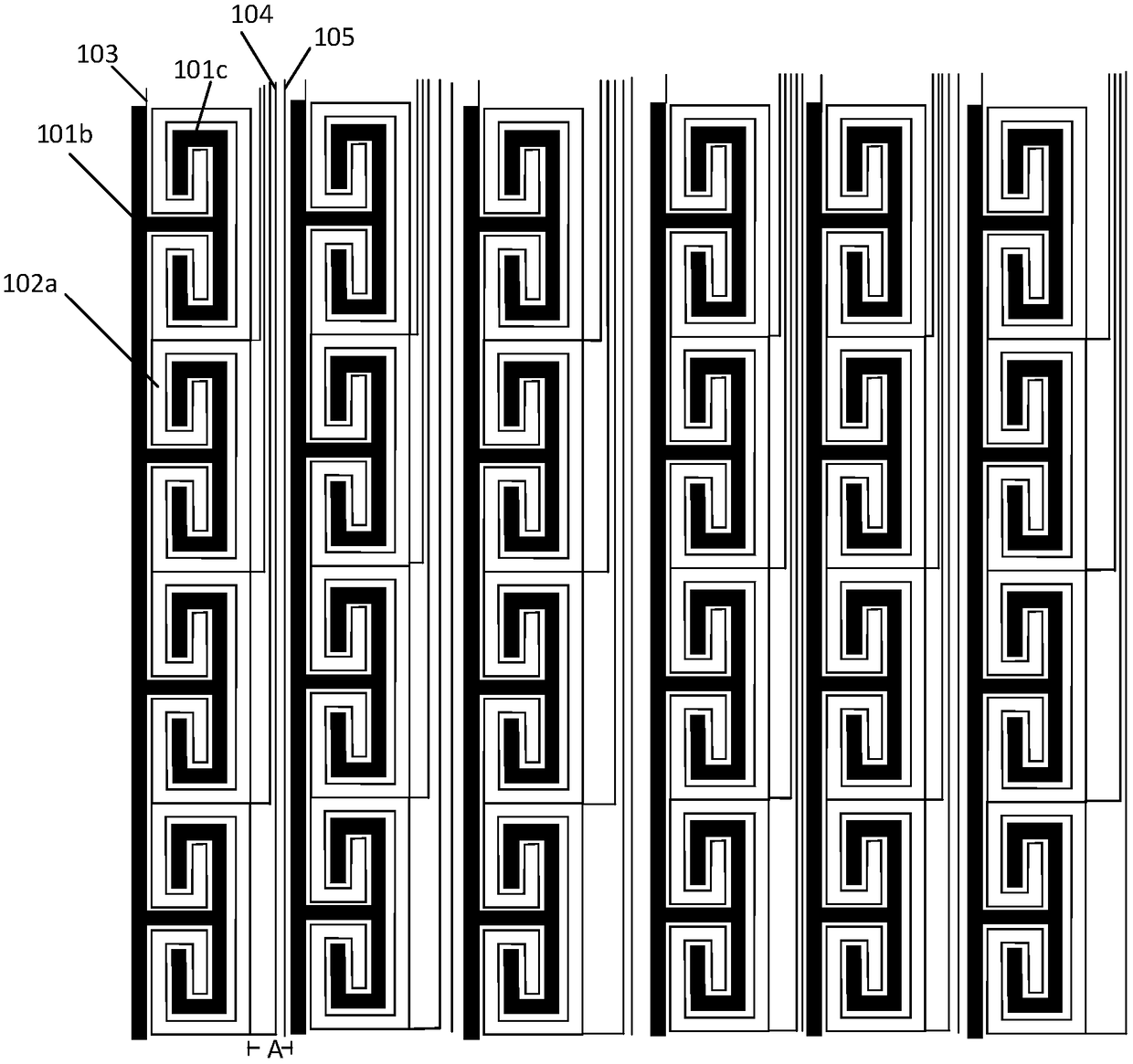
[0028] refer to Figure 1-Figure 3 , this embodiment provides a touch panel, including a substrate and a touch IC (not shown in the figure), the substrate is provided with a plurality of columns of first touch electrode units 101 and a plurality of second touch electrode units 102, Multiple columns of first touch electrode units 101 and multiple second touch electrode units 102 are arranged on the same layer;

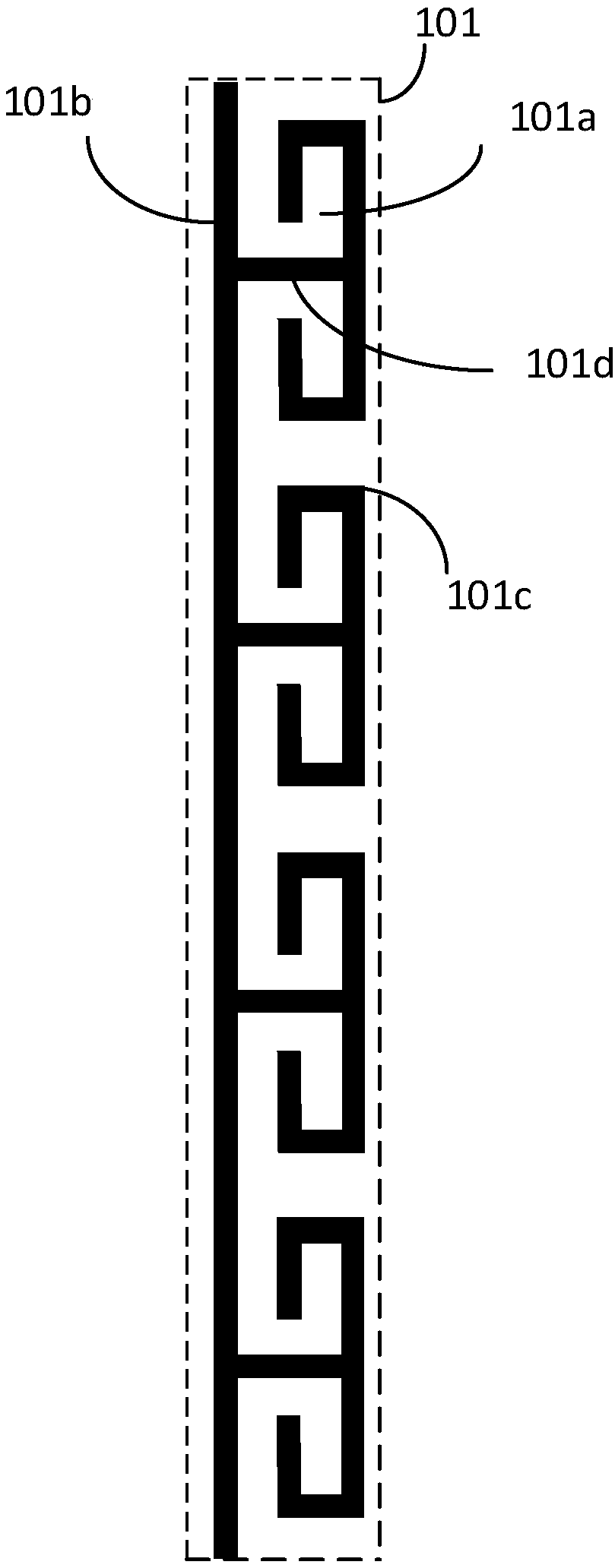
[0029] The first touch electrode unit includes a first conductive portion and a first hollow portion 101a, the first conductive portion includes a strip-shaped conductive portion 101b and a plurality of bent conductive portions 101c, the multiple bent conductive portions 101c and the strip-shaped conductive portion 101b connect;

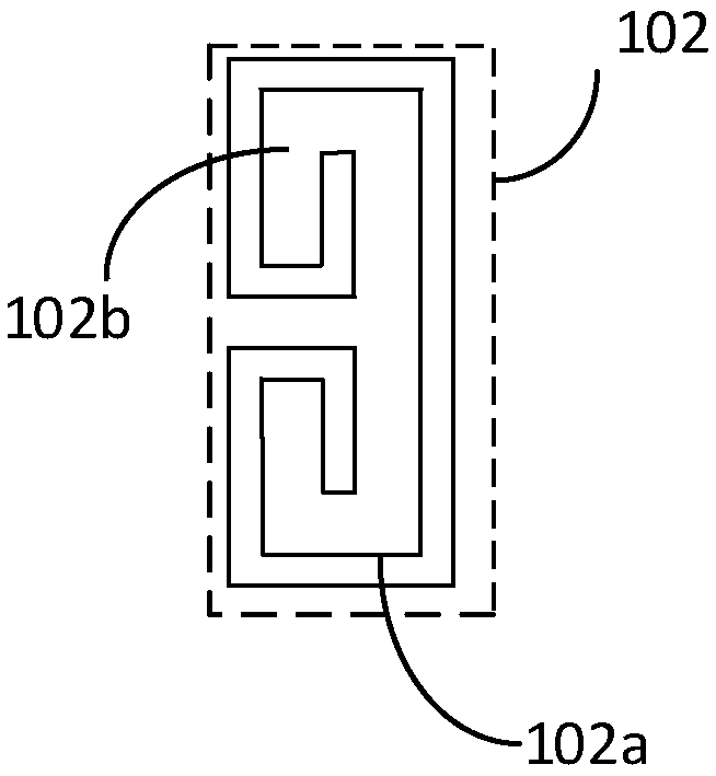
[0030] The second touch electrode unit 102 includes a second conductive part 102a and a second hollow part 102b, the second conductive part 102a is a bent structure, the second conductive part 102a and the bent conductive part 101c interpenet...

Embodiment 2

[0055] This embodiment provides a display device, including the touch panel as described in the first embodiment.

[0056] The display device may be any product or component with a display function such as a mobile phone, a tablet computer, a monitor, a notebook computer, and the like.


PUM

PropertyMeasurementUnit
Widthaaaaaaaaaa

Abstract

The invention provides a touch panel and a display device. The touch panel comprises a substrate and a touch IC. A plurality of columns of first touch electrode units and a plurality of second touch electrode units are arranged on the substrate, and are arranged at the same layer. The first touch electrode unit includes a first conductive portion and a first hollow-out portion, the first conductive portion including a strip-shaped conductive portion and a plurality of bent conductive portions, the plurality of bent conductive portions being connected with the strip-shaped conductive portions;The second touch electrode unit comprises a second conductive part and a second hollow-out part, wherein the second conductive part is a bent structure, the second conductive part and the bent conductive part intersect each other, and the second conductive part corresponds to the first hollow-out part, and the bent conductive part corresponds to the second hollow-out part; The plurality of columnsof first touch electrode units and the plurality of second touch electrode units are arranged on the same layer, and the single-layer structure can effectively reduce the production cost of the touchpanel.

Description

technical field [0001] The present invention relates to the field of touch technology, in particular to a touch panel and a display device. Background technique [0002] With the development of electronic technology, touch screens are more and more widely used. The touch chip extracts possible touch information by reading the data fed back from the touch screen. The data fed back by the touch screen consists of an M*N matrix, where M represents the number of signal sending ends (excitation ends), and N represents the number of signal receiving ends. Each sending end and receiving end constitute a capacitive sensor (self-capacitance or mutual capacitance). The change of this capacitive sensor is converted into a value through a certain circuit, stored in the corresponding position in the M*N matrix, and analyzed by the touch chip. and processing. The basic condition for judging the touch is: there is a value exceeding the preset threshold (defined as the touch threshold, ob...

Claims


Application Information

Patent Timeline
IPC IPC(8): G06F3/041G06F3/044
CPCG06F3/0412G06F3/044
Inventor 李虎李鹏
Owner SHENZHEN DEMINGLI ELECTRONICS
Why Eureka
Try Eureka