Array substrate and preparation method thereof, display panel and display device

An array substrate and substrate substrate technology, which is applied in the manufacture of semiconductor/solid-state devices, electrical components, diodes, etc., can solve the problem of large attenuation of light brightness, and achieve the effects of improving contrast, increasing maximum brightness, and reducing absorption

Active Publication Date: 2019-01-25
BOE TECH GRP CO LTD
View PDF4 Cites 30 Cited by
  • Summary
  • Abstract
  • Description
  • Claims
  • Application Information

AI Technical Summary

Problems solved by technology

[0006] Embodiments of the present invention provide an array substrate and a preparation method thereof, a display panel, and a display device, w

Method used


Image

  • Array substrate and preparation method thereof, display panel and display device
  • Array substrate and preparation method thereof, display panel and display device
  • Array substrate and preparation method thereof, display panel and display device

Examples


Embodiment Construction

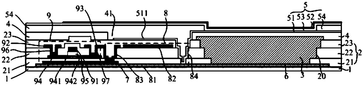
[0027] The following will clearly and completely describe the technical solutions in the embodiments of the present invention with reference to the accompanying drawings in the embodiments of the present invention. Obviously, the described embodiments are only some, not all, embodiments of the present invention. Based on the embodiments of the present invention, all other embodiments obtained by persons of ordinary skill in the art without making creative efforts belong to the protection scope of the present invention.

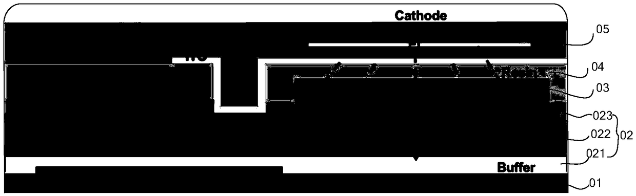
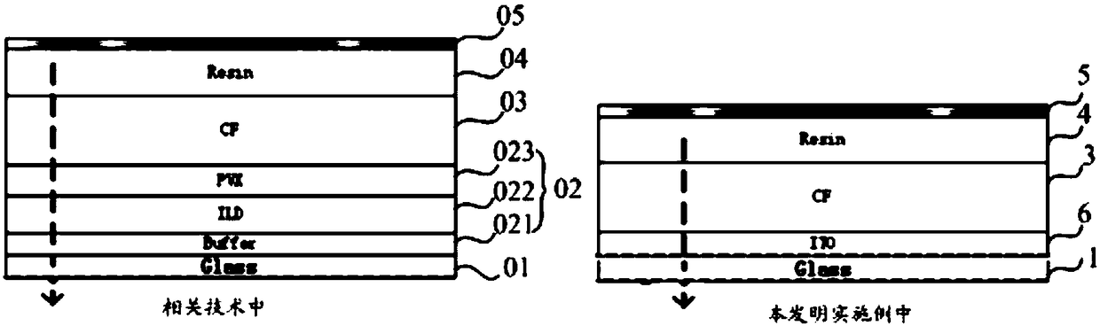
[0028] In describing the present invention, it is to be understood that the terms "center", "upper", "lower", "front", "rear", "left", "right", "vertical", "horizontal", The orientations or positional relationships indicated by "top", "bottom", "inner", "outer", etc. are based on the orientations or positional relationships shown in the drawings, and are only for the convenience of describing the present invention and simplifying the description, rather than in...


PUM


Abstract

The invention discloses an array substrate and a preparation method thereof, a display panel and a display device, which relate to the technical field of display and are invented for solving the problem that the brightness of the light emitted by an organic light emitting unit in the array substrate in the related art is attenuated greatly. The array substrate, include multiple pixels, each of thepixels includes a plurality of sub-pixels, for each of the sub-pixels, the sub-pixel includes a substrate, an insulating layer, a color filter layer, a flat layer and an organic light emitting unit,At least a part of that color filtering layer is filled in the first opening; the flat layer covers the insulate layer and covers the surface of the color filter layer; and the organic light emittingunit is arranged on the flat layer. The invention can be used in an OLED display device.

Description

technical field [0001] The present invention relates to the field of display technology, in particular to an array substrate and a preparation method thereof, a display panel, and a display device. Background technique [0002] Organic Light Emitting Display (OLED) has the advantages of white light emission, low driving voltage, high luminous efficiency, short response time, high definition and contrast, nearly 180-degree viewing angle, and wide operating temperature range. It can realize flexible display and large It is recognized by the industry as a display device with the most potential for development due to its many advantages such as full-color display. [0003] Among them, contrast is an important indicator of OLED, and a higher contrast can bring users a good visual experience; the contrast of a display device is: in a dark room, the brightness under the white screen (at its brightest) is divided by the black screen (at darkest) the value obtained from the brightne...

Claims


Application Information

Patent Timeline
IPC IPC(8): H01L27/32H01L21/77
CPCH10K59/00H10K59/38H10K59/12H10K59/1201H10K59/123H10K59/124H10K59/1213H10K59/1216H10K59/126H10K50/85
Inventor 宋振王国英
Owner BOE TECH GRP CO LTD
Why Eureka
Try Eureka