

Array substrate, its preparation method, display panel, device and pixel driving circuit
A technology for array substrates and display panels, applied to circuits, electrical components, static indicators, etc., can solve the problems of reduced visual effects, single display mode of display technology, etc.
- Summary
- Abstract
- Description
- Claims
- Application Information
AI Technical Summary
Problems solved by technology
Method used
Image

Examples
Embodiment Construction
[0045] The application will be further described in detail below in conjunction with the accompanying drawings and embodiments. It should be understood that the specific embodiments described here are only used to explain related inventions, rather than to limit the invention. It should also be noted that, for ease of description, only parts related to the invention are shown in the drawings.
[0046] It should be noted that, in the case of no conflict, the embodiments in the present application and the features in the embodiments can be combined with each other.
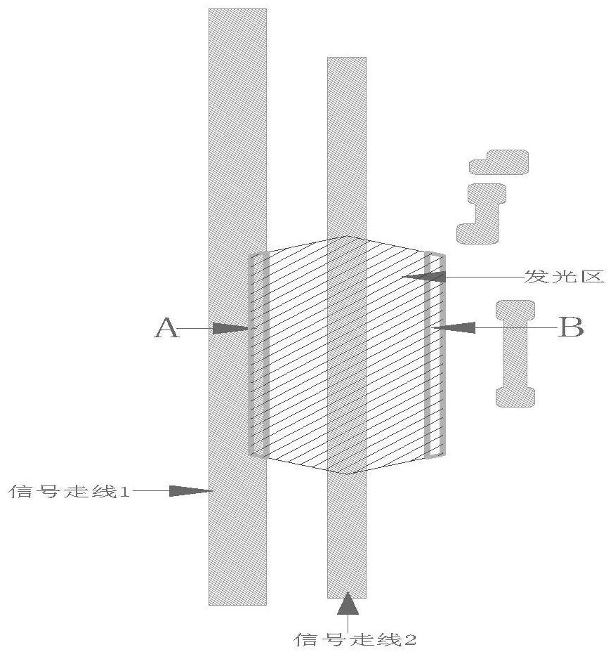
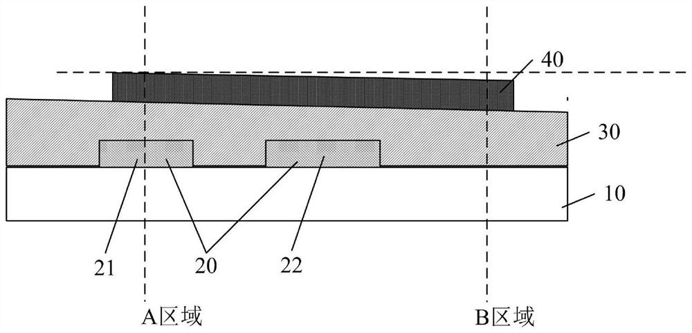
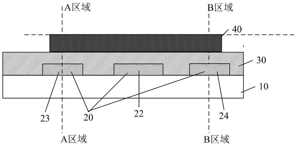
[0047] First, if figure 1 and figure 2 As shown in FIG. 2 , they are a top view and a cross-sectional view of an arrangement mode of the wiring layer of the array substrate, respectively.
[0048] refer to figure 1 and figure 2 , in the pixel structure arranged in GGRB, the signal wiring 1 is located under the A area of the light emitting layer 40, the signal wiring 2 is located below the center line of the...
PUM
 Abstract
Description
Claims
Application Information