Display substrate and manufacturing method thereof, display panel and display device

A display substrate and display panel technology, applied in semiconductor devices, electrical components, circuits, etc., can solve the problems of ACF bubbles, ACF difficult to compress, etc., and achieve the effect of avoiding bubbles and ensuring electrical connection performance

Active Publication Date: 2019-06-07
BOE TECH GRP CO LTD +1
View PDF3 Cites 11 Cited by
  • Summary
  • Abstract
  • Description
  • Claims
  • Application Information

AI Technical Summary

Problems solved by technology

[0005] In order to solve the problem in the related art that the ACF between the OLED panel and the driver IC is difficult to flatten, resulting in bubbles in the ACF, an embodiment of the present invention provides a display substrate and a manufacturing method thereof, a display panel, and a display device

Method used


Image

  • Display substrate and manufacturing method thereof, display panel and display device
  • Display substrate and manufacturing method thereof, display panel and display device
  • Display substrate and manufacturing method thereof, display panel and display device

Examples


Embodiment Construction

[0035] In order to make the object, technical solution and advantages of the present invention clearer, the implementation manner of the present invention will be further described in detail below in conjunction with the accompanying drawings.

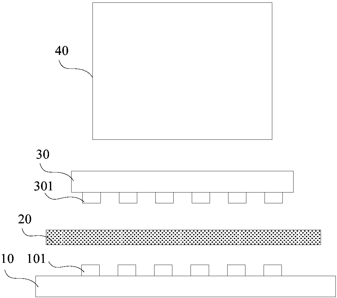
[0036] In order to facilitate the description later, the following will be combined with the attached figure 1 The OLED panel Bonding involved in the embodiment of the present invention is explained:

[0037] figure 1 It is a schematic diagram of Bonding of the OLED panel, see figure 1 , wherein the label 10 is the display substrate (that is, the OLED substrate), 20 is the ACF, and 30 is the driver IC. During Bonding, ACF 20 is coated on the bonding area of ​​the display substrate 10, and then, under the action of the heater 40, the driver IC 30 is pressed onto the display substrate 10 , and the pad 101 of the display substrate 10 and the pad 301 of the driving IC 30 are conducted under the action of the ACF 20 .

[0038] However, w...


PUM


Abstract

The invention discloses a display substrate and a manufacturing method thereof, a display panel and a display device, and belongs to the field of displays. The display substrate includes a bonding area, a plurality of bonding pads arranged at intervals are arranged at the bonding area, the bonding pads are separated from one another through an insulation layer, and the insulation layer between atleast two adjacent bonding pads is provided with a groove. The insulation layer between at least two adjacent bonding pads is provided with the groove to allow an ACF (Anisotropic Conductive Film) toflow to the grooves when pressing-down of the ACF is performed to ensure the uniform distribution of the ACFs between the at least two adjacent Pads so as to solve the unfairness caused by difficult ACF glue discharge between the display substrate and a drive IC (Integrated Circuit), avoid a condition that bubbles are generated due to unfairness of the ACFs and ensure the electrical connection performance between the display substrate and the drive IC.

Description

technical field [0001] The invention relates to the field of displays, in particular to a display substrate and a manufacturing method thereof, a display panel, and a display device. Background technique [0002] In recent years, an organic light-emitting diode (Organic Light-Emitting Diode, OLED for short) display has attracted more and more attention from the industry due to its excellent performance. Compared with the liquid crystal display (English Liquid Crystal Display, referred to as LCD) which currently occupies the main market, OLED display has a series of advantages such as light weight, small thickness, low power consumption, bright color, fast response speed, wide viewing angle, and flexible display. advantage. [0003] Bonding (English Bonding) is an important step in the OLED display process. Bonding refers to the bonding of the pads (English Pad) in the Bonding area of ​​the OLED panel (English Panel) and the driver during the production process of the OLED d...

Claims


Application Information

Patent Timeline
Patent Type & Authority Applications(China)
IPC IPC(8): H01L27/32
CPCH10K59/124H10K59/131H10K50/80H10K71/00H10K59/1201
Inventor 辛燕霞阳智勇陈飞
Owner BOE TECH GRP CO LTD
Why Eureka
Try Eureka