

Semiconductor lead frame stacking device
A lead frame and semiconductor technology, which is applied in semiconductor/solid-state device manufacturing, transportation and packaging, electrical components, etc., can solve the problems of low production efficiency and manpower consumption, and achieve the effects of reducing production costs, saving labor, and avoiding artificial addition
- Summary
- Abstract
- Description
- Claims
- Application Information
AI Technical Summary
Problems solved by technology
Method used
Image

Examples
Embodiment
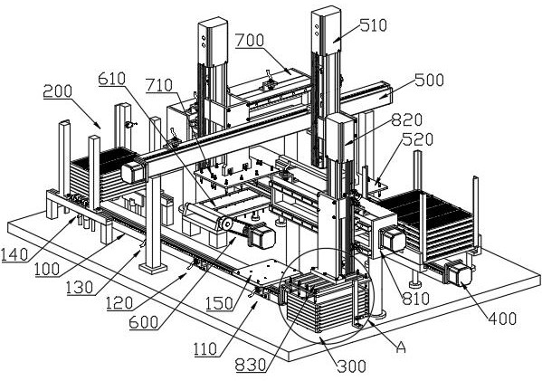
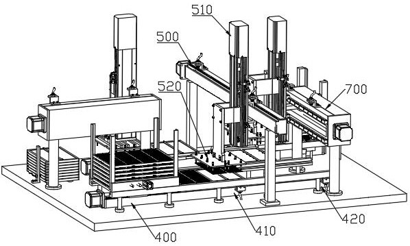
[0048] Such as Figure 1 to Figure 7 As shown, a semiconductor lead frame stacking device includes: a first linear mechanism 100, a stacking mechanism 200, a pad buffer mechanism 300, a second linear mechanism 400, a third linear mechanism 500, a rotating mechanism 600 and a first Four linear mechanism 700.
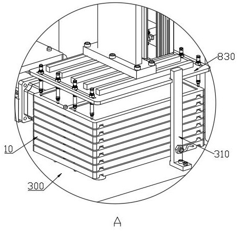
[0049] Specifically, the first linear mechanism 100 has a stacking mechanism 200 at one end and a pad buffer mechanism 300 at the other end for stacking empty pads. One end of the stacking mechanism 200 is sequentially provided with a pad mounting station 110, a first assembly station 120, a second assembly station 130, and a finished product stacking station 140, and the stacking mechanism 200 is arranged above the finished product stacking station 140. The linear mechanism 100 is slidably provided with a running plate 150. The running plate 150 is used to install and transfer the pad 10. The top surface of the pad 10 is used to carry the bottom lead frame, correspondin...
PUM
 Abstract
Description
Claims
Application Information