

Design method of parameterized customized transistor layout and chip layout structure
A design method and technology of layout structure, applied in the field of electronic information, can solve the problems of non-optimal area, poor versatility, and failure to consider the layout of layout design, etc., so as to reduce visual fatigue, make layout units concise and clear, and improve layout design efficiency effect
- Summary
- Abstract
- Description
- Claims
- Application Information
AI Technical Summary
Problems solved by technology
Method used
Image

Examples
Embodiment Construction
[0023] In order to make the purpose, technical solutions and advantages of the embodiments of the present invention more clear, the following will clearly and completely describe the technical solutions of the embodiments of the present invention in conjunction with the drawings of the embodiments of the present invention. Apparently, the described embodiments are some, not all, embodiments of the present invention. Based on the described embodiments of the present invention, all other embodiments obtained by persons of ordinary skill in the art without creative efforts shall fall within the protection scope of the present invention.
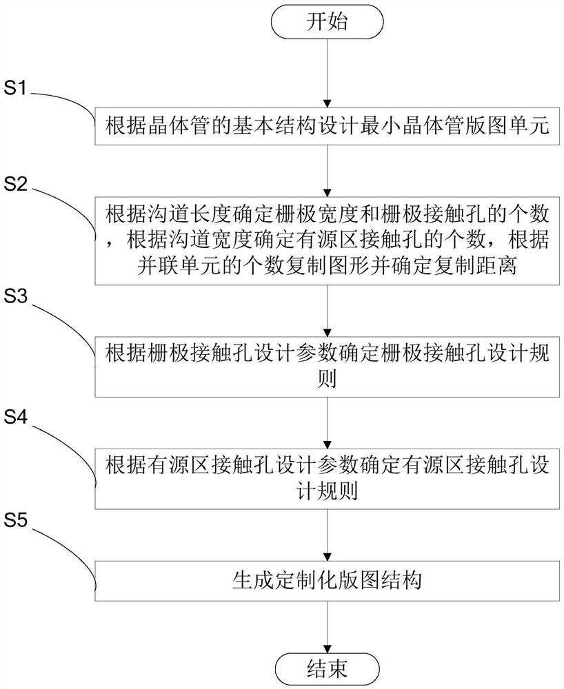
[0024] see figure 1 , a method for designing a parametric custom transistor layout according to the present invention, when generating a customized transistor layout unit according to the basic structure and parameterized selection of the transistor, specifically includes the following steps:
[0025] First, step S1 is performed to design the m...
PUM
 Abstract
Description
Claims
Application Information