Plasma display device

a technology of plasma and display device, which is applied in the field of plasma display device, can solve the problems of deteriorating display quality, large amount of current carried momentarily, and distortion of the voltage waveform of the sustain pulse, so as to prevent the deterioration of residual image caused by increase of luminance level, the effect of preventing the variation of discharge intensity

Inactive Publication Date: 2007-03-15
PANASONIC CORP
View PDF4 Cites 11 Cited by
  • Summary
  • Abstract
  • Description
  • Claims
  • Application Information

AI Technical Summary

Benefits of technology

[0008] An object of the present invention is to provide a plasma display device capable of improving a residual image caused by increase of a luminance level while preventing variation in discharge intensity in each display cell.
[0010] In the plasma display device of the present invention, the pause period between the sustain pulse application end point at which one sustain pulse is applied in the sustain period of each of the subfields and the sustain pulse application starting point at which the next sustain pulse is applied is changed in accordance with an average luminance level of the video signal. Accordingly, deterioration of a residual image caused by increase of a luminance level can be prevented while preventing variation in discharge intensity in each display cell.

Problems solved by technology

In the sustain stage, in the case where many display cells are set in the lighting state and a sustain pulse is applied to generate discharge in many cells almost at the same time, a large amount of current is carried momentarily, and distortion occurs in the voltage waveform of the sustain pulse.
Consequently, in accordance with a slight shift in a time point to start discharge, the voltage value being applied in discharge is varied in each of the display cells, variation occurs in discharge intensity, and thus display quality might be deteriorated.
As a result, the level of luminance increases, so that residual image effect might become large.

Method used


Image

  • Plasma display device
  • Plasma display device
  • Plasma display device

Examples


Embodiment Construction

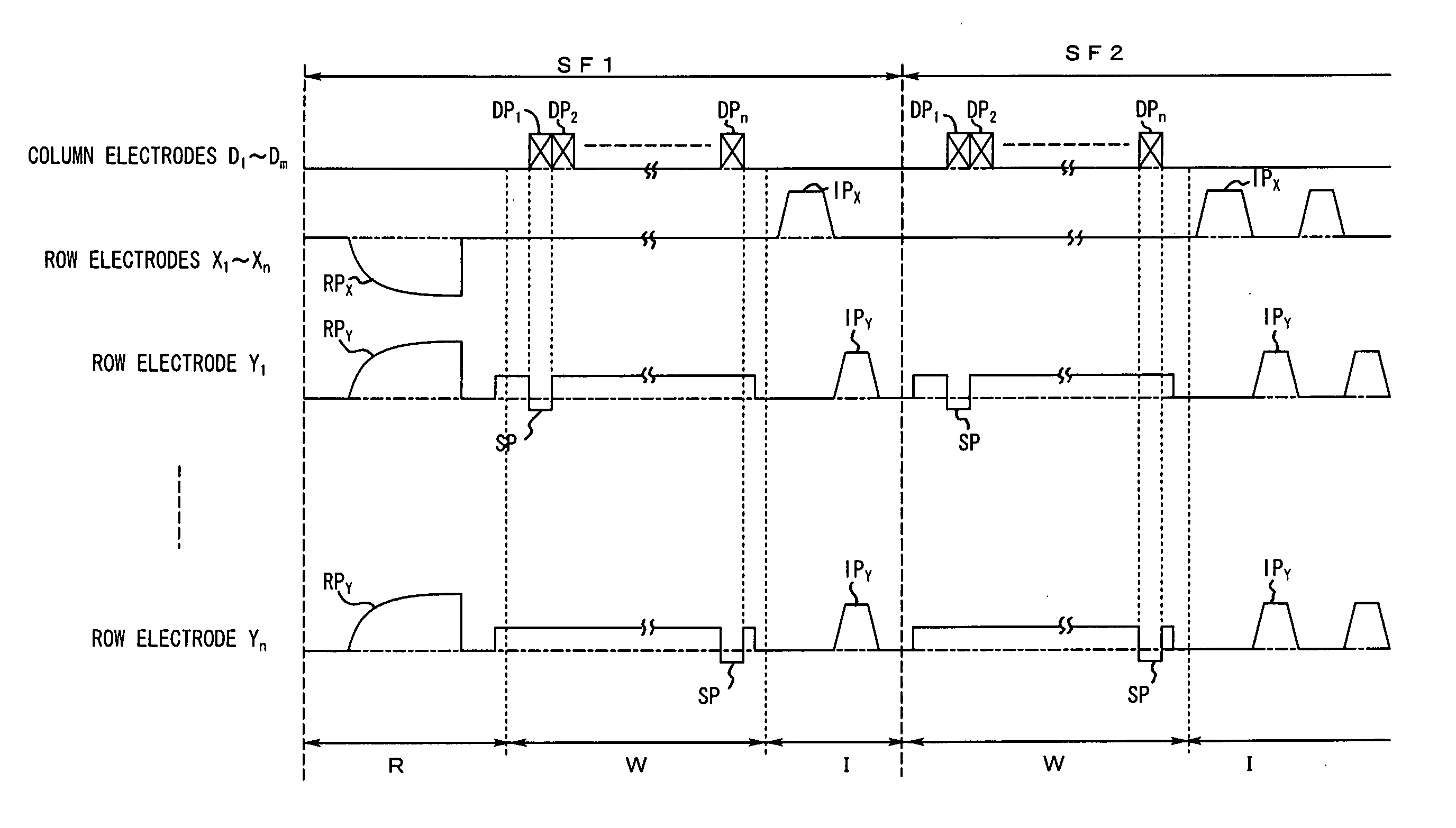
[0030] Hereinafter, an embodiment according to the present invention will be described in detail with reference to the drawings.

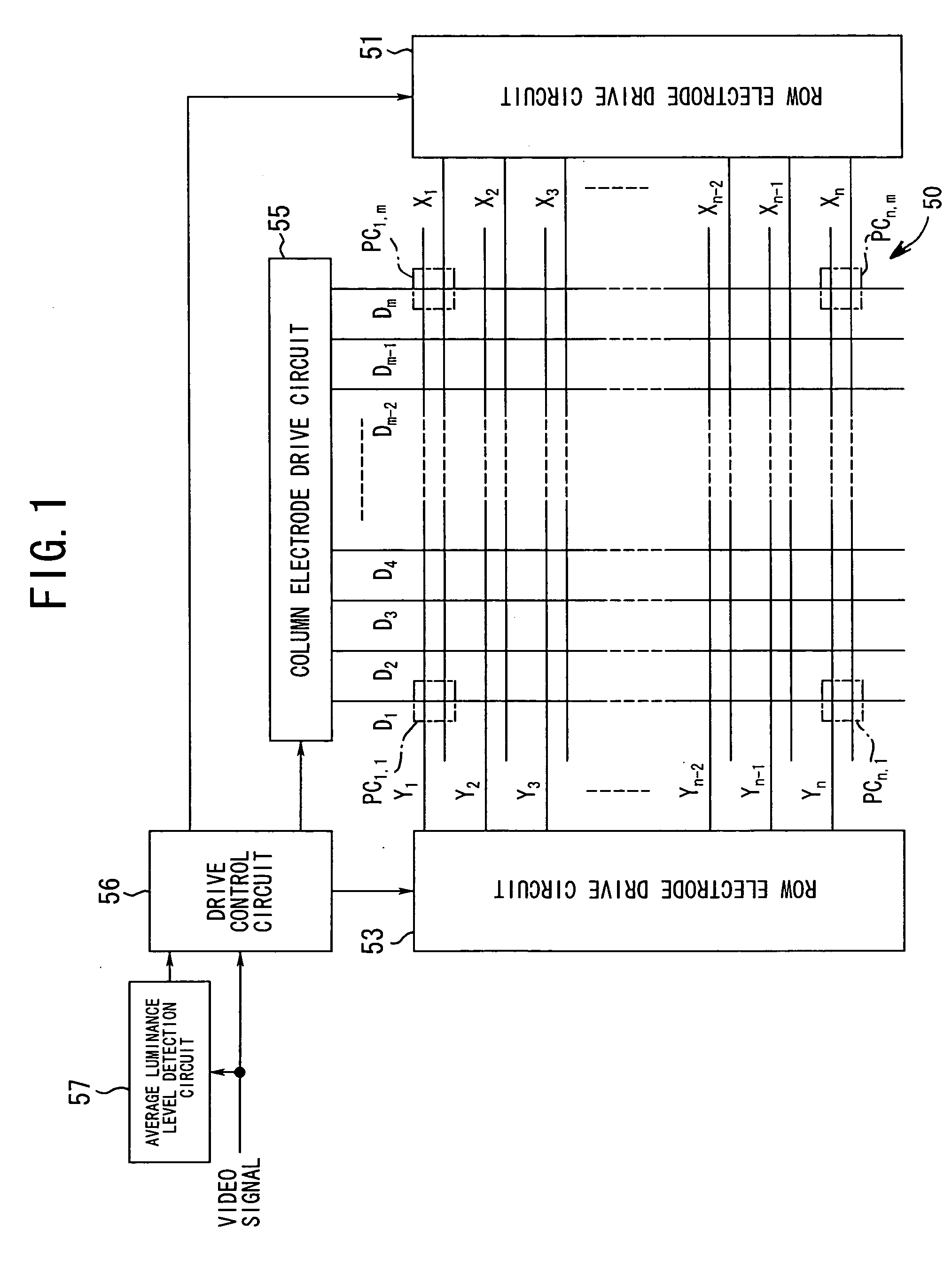
[0031]FIG. 1 is a diagram illustrating an outline configuration of a plasma display device according to the invention.

[0032] As shown in FIG. 1, the plasma display device is configured of a PDP 50 as a plasma display panel, an X-row electrode drive circuit 51, a Y-row electrode drive circuit 53, a column electrode drive circuit 55, a drive control circuit 56, and an average luminance level detection circuit 57.

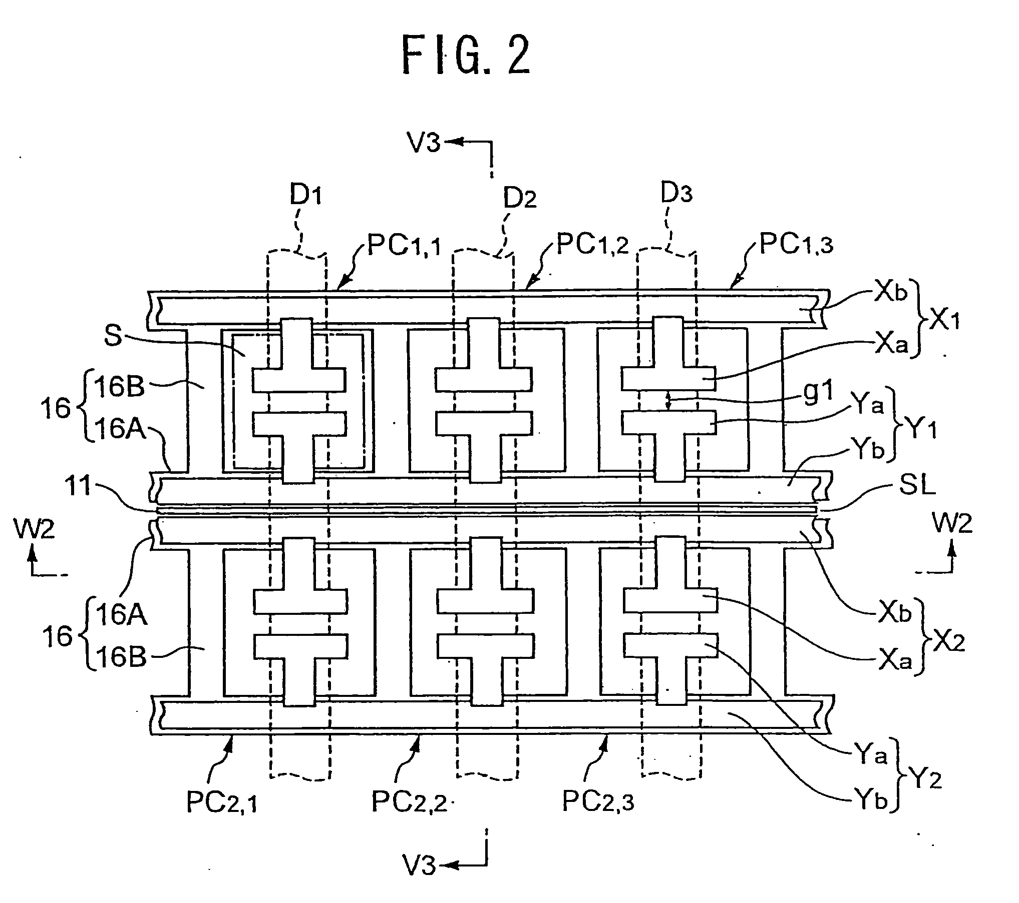
[0033] In the PDP 50, column electrodes D1 to Dm are extended and arranged in the longitudinal direction (vertical direction) of a two-dimensional display screen, and row electrodes X1 to Xn and row electrodes Y1 to Yn are extended and arranged in the lateral direction (the horizontal direction) thereof. The row electrodes X1 to Xn and row electrodes Y1 to Yn form row electrodes pairs (Y1, X1), (Y2, X2), (Y3, X3), . . . , (Yn, Xn) which are paired ...


PUM


Abstract

A plasma display device which changes, in accordance with an average luminance level of a video signal, the length of a pause period between a sustain pulse application end point at which one sustain pulse is applied in a sustain period of each of subfields and a sustain pulse application starting point at which the next sustain pulse is applied.

Description

BACKGROUND OF THE INVENTION [0001] 1. Field of the Invention [0002] The present invention relates to a plasma display device using a plasma display panel. [0003] 2. Description of the Related Art [0004] Currently, as a thin display device, an AC type (alternating discharge type) plasma display panel becomes commercially available. In the plasma display panel, two substrates, that is, a front glass substrate and a rear glass substrate are disposed with a predetermined space as faced to each other. On the inner surface (the surface facing the rear glass substrate) of the front glass substrate as a display surface, multiple row electrode pairs are formed as sustain electrode pairs, which are paired with each other and extended in parallel. On the rear glass substrate, multiple column electrodes are extended and formed as address electrodes as intersecting with the row electrode pairs, and are coated with a fluorescent material. When seen from the display surface side, a display cell co...

Claims


Application Information

Patent Timeline
Patent Type & Authority Applications(United States)
IPC IPC(8): G09G3/28G09G3/288G09G3/20G09G3/291G09G3/294G09G3/296G09G3/298H01J11/12H01J11/22H01J11/24H01J11/26H01J11/34H01J11/36H01J11/38H01J11/40H01J11/42H01J11/44H01J11/50H04N5/66
CPCG09G3/294G09G3/2944G09G3/2965H01J2211/40G09G2320/0257G09G2320/043G09G2360/16G09G2320/0233G09G3/293G09G3/296
Inventor SATO, YOSHICHIKAIKEDA, MOTOFUMIONIZUKA, MASATSUGU
Owner PANASONIC CORP
Why Eureka
Try Eureka