Liquid crystal display device

a display device and liquid crystal technology, applied in non-linear optics, instruments, optics, etc., can solve the problems of reducing display quality or reliability, prone to easy generation of bubbles in the inside of the display panel, and enhancing the adhesion strength, enhancing the adhesiveness, and excellent advantageous effects

Active Publication Date: 2008-08-14
PANASONIC LIQUID CRYSTAL DISPLAY CO LTD +1
View PDF6 Cites 18 Cited by
  • Summary
  • Abstract
  • Description
  • Claims
  • Application Information

AI Technical Summary

Benefits of technology

[0021]According to the present invention, the adhesion area between one substrate and the second organic resin film below the sealing-material-applied region is enlarged and hence, an adhesion strength between one substrate and the stacked film over one substrate can be enhanced. Further, by forming unevenness on a film surface of the second organic resin film, the adhesion area between the second organic resin film and the sealing material is enlarged thus enhancing the adhesion strength on an adhesive interface between the second organic resin film and the sealing material. Accordingly, the adhesiveness can be largely enhanced and hence, the interface peeling-off hardly occurs whereby the generation of bubbles in the inside of the liquid crystal display panel can be eliminated thus giving rise to an extremely excellent advantageous effect that a liquid crystal display device of high quality and reliability can be realized.

Problems solved by technology

However, due to peeling-off of the black matrix film on an interface between the electrode substrate and a light shielding film, bubbles are liable to be easily generated in the inside of the display panel thus giving rise to drawbacks such as lowering of display quality or lowering of reliability.
However, in the same manner as the above-mentioned liquid crystal display panel, due to peeling-off of the black matrix film on an interface between the electrode substrate and a light shielding film, there exists a drawback that bubbles are liable to be easily generated in the inside of a display panel.
However, there exists a drawback that a gap becomes unstable in a sealing material applying portion due to the influence of a stepped portion of the overcoat film.

Method used


Image

  • Liquid crystal display device
  • Liquid crystal display device
  • Liquid crystal display device

Examples


embodiment 1

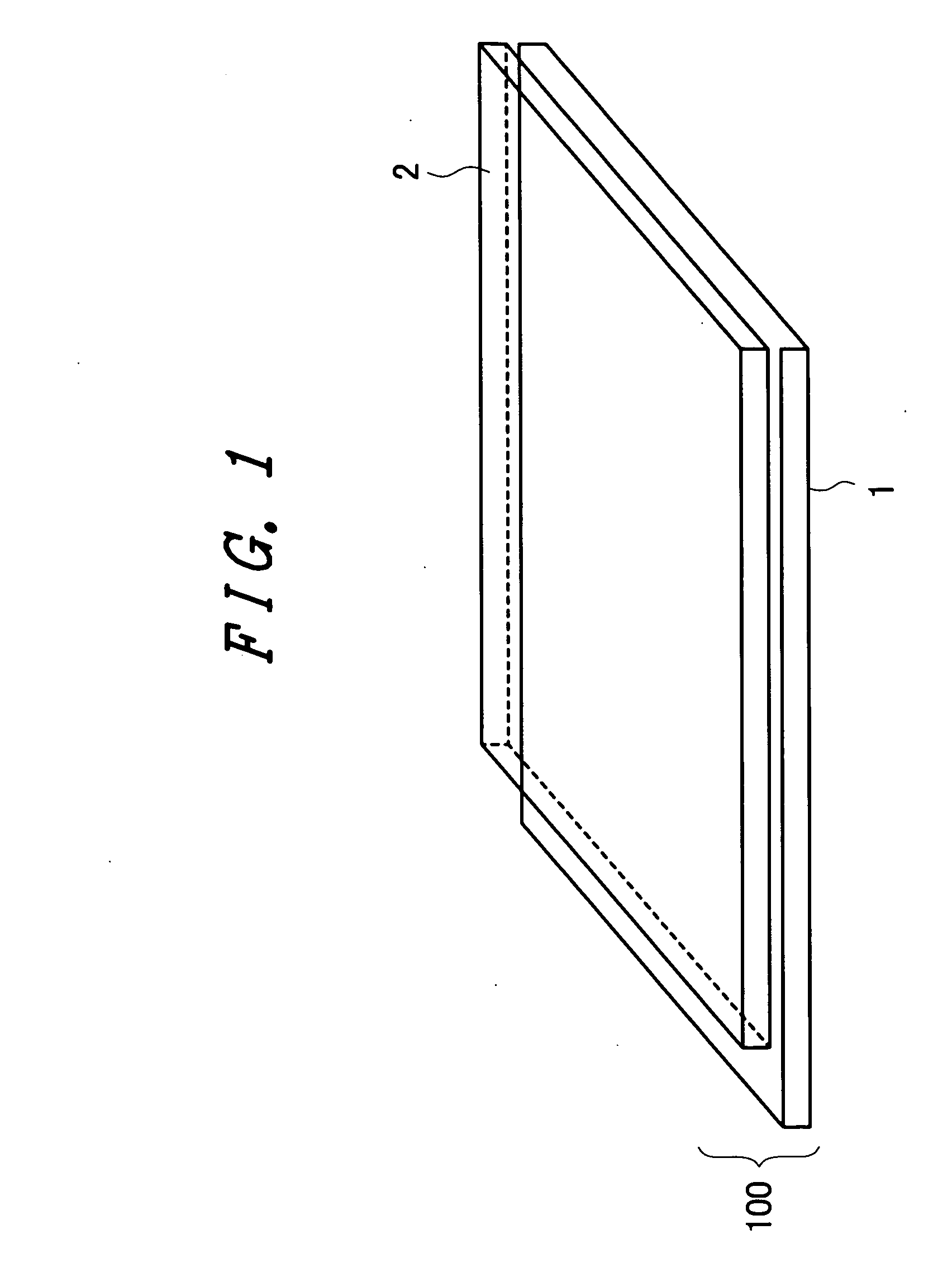
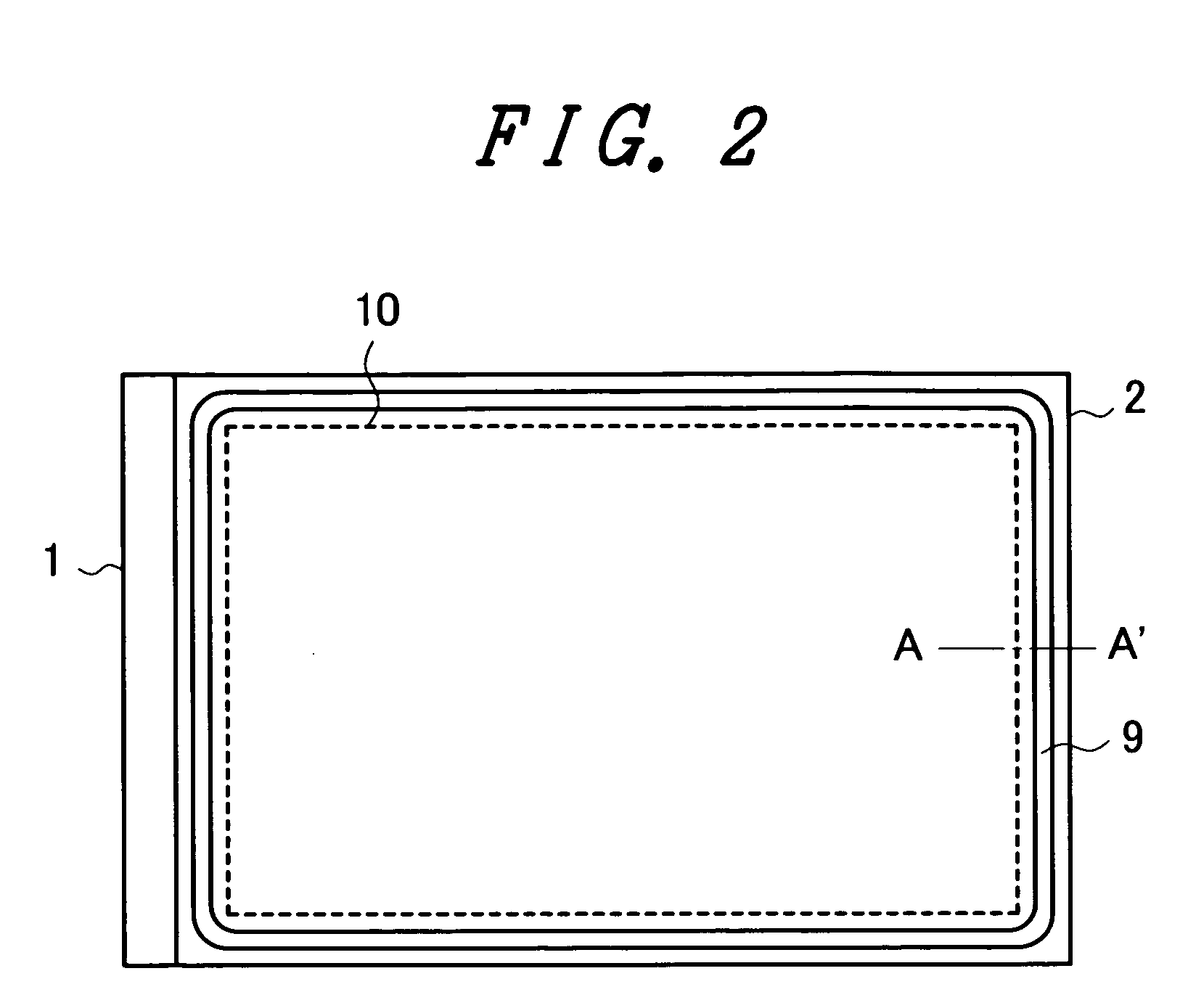
[0037]FIG. 1 is a schematic perspective view of an essential part for explaining the constitution of a liquid crystal display panel for explaining one embodiment of a liquid crystal display device according to the present invention. FIG. 2 is a schematic plan view of an essential part as viewed from above showing the constitution in FIG. 1. FIG. 3 is an enlarged cross-sectional view of an essential part of a sealing portion taken along a line A-A′ in FIG. 2. FIG. 4A to FIG. 4C are schematic constitutional views of an essential part of the sealing portion showing the constitution of the liquid crystal display panel, wherein FIG. 4A is a cross-sectional view of the sealing portion in FIG. 3, FIG. 4B is a plan view of a glass substrate in FIG. 4A as viewed from an inner surface side, and FIG. 4C is a perspective view of an essential part in FIG. 4B. In all of the above-mentioned drawings, same symbols are given to identical parts and their explanations are omitted when unnecessary.

[003...

embodiment 2

[0051]FIG. 6 is an enlarged cross-sectional view of an essential part of a sealing portion taken along a line A-A′ in FIG. 2 for explaining the constitution of a liquid crystal display panel for explaining another embodiment of a liquid crystal display device according to the present invention. FIG. 7A to FIG. 7C are schematic constitutional views of an essential part of the sealing portion showing the constitution of the liquid crystal display panel, wherein FIG. 7A is a cross-sectional view of the sealing portion in FIG. 6, FIG. 7B is a plan view of a glass substrate in FIG. 7A as viewed from an inner surface side, and FIG. 7C is a perspective view of an essential part in FIG. 7B. In all of the above-mentioned drawings, same symbols are given to identical parts and their explanations are omitted when unnecessary.

[0052]In FIG. 6 and FIG. 7, the liquid crystal display panel 100 is constituted different from the liquid crystal display panel 100 of the embodiment 1 in the following po...


PUM

PropertyMeasurementUnit
widthaaaaaaaaaa
electric fieldaaaaaaaaaa
adhesion strengthaaaaaaaaaa

Abstract

The present invention provides a liquid crystal display device which can enhance quality and reliability of image display by preventing the generation of bubbles in the inside of a liquid crystal display panel and, at the same time, by suppressing leaking of light from an end of a black matrix film. In the liquid crystal display panel which sandwiches a liquid crystal layer between two glass substrates, the liquid crystal layer is surrounded by a sealing material having a predetermined width. On one glass substrate, a black matrix film and an overcoat film are arranged from one-glass-substrate side such that the black matrix film and the overcoat film overlap the sealing material. The black matrix film is, in the widthwise direction of the sealing material, formed into a planar flat black matrix film until a middle position of the sealing material from a side on which the liquid crystal layer is arranged, and is formed into a slit-shaped slit black matrix film from the middle position. Due to such a constitution, an adhesion area between the glass substrate and the overcoat film under an applied region of the sealing material is enlarged and hence, an adhesion strength is increased thus largely enhancing an adhesion strength.

Description

CROSS-REFERENCE TO RELATED APPLICATIONS[0001]The disclosure of Japanese Patent Application No. 2007-11933 filed on Jan. 22, 2007 including the specification, drawings and abstract is incorporated herein by reference in its entirety.BACKGROUND OF THE INVENTION[0002]1. Field of the Invention[0003]The present invention relates to a liquid crystal display device having a liquid crystal display panel which sandwiches a liquid crystal layer between a pair of substrates, and more particularly to the stacked structure of an organic resin film on a peripheral portion between a pair of substrates which is arranged to face each other in an opposed manner.[0004]2. Description of the Related Art[0005]A liquid crystal display device having a liquid crystal display panel is an image display device which is basically configured by sealing a liquid crystal layer between two substrates consisting of a first substrate and a second substrate preferably formed of a glass substrate respectively, and perf...

Claims


Application Information

Patent Timeline
Patent Type & Authority Applications(United States)
IPC IPC(8): G02F1/1339G02F1/1335
CPCG02F1/1339
Inventor NAKAGAWA, SHIGEO
Owner PANASONIC LIQUID CRYSTAL DISPLAY CO LTD
Why Eureka
Try Eureka