Organic semiconductor device, display using same, and imager

a technology of organic semiconductors and semiconductor components, applied in thermoelectric devices, television systems, radio control devices, etc., can solve the problems of difficult design of desired configurations, change of light emitting/receiving characteristics, and difficulty in proper selection of materials, so as to achieve electron-hole recombination or photoelectric conversion in organic semiconductors.

Inactive Publication Date: 2009-08-27
KYOTO UNIV +2
View PDF1 Cites 15 Cited by
  • Summary
  • Abstract
  • Description
  • Claims
  • Application Information

AI Technical Summary

Benefits of technology

[0006]It is an object of the present invention to provide an organic semiconductor device which effectively allows electron-hole recombination or photoelectric conversion in organic semiconductor.

Problems solved by technology

In practice, however, the proper selection of the materials still remains difficult.
However, it is difficult to design a configuration of desired characteristics.
Further, in the cases mentioned above, neither the device that emits light nor the device that detects light can change the light emitting / receiving characteristics.

Method used


Image

  • Organic semiconductor device, display using same, and imager
  • Organic semiconductor device, display using same, and imager
  • Organic semiconductor device, display using same, and imager

Examples


Embodiment Construction

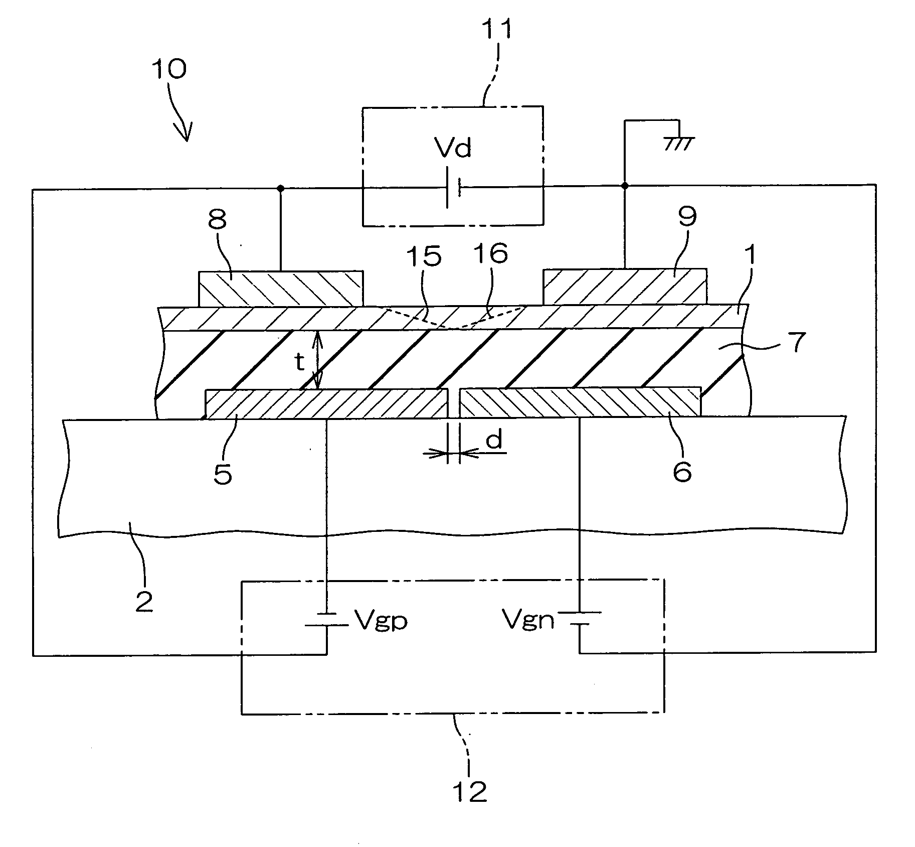
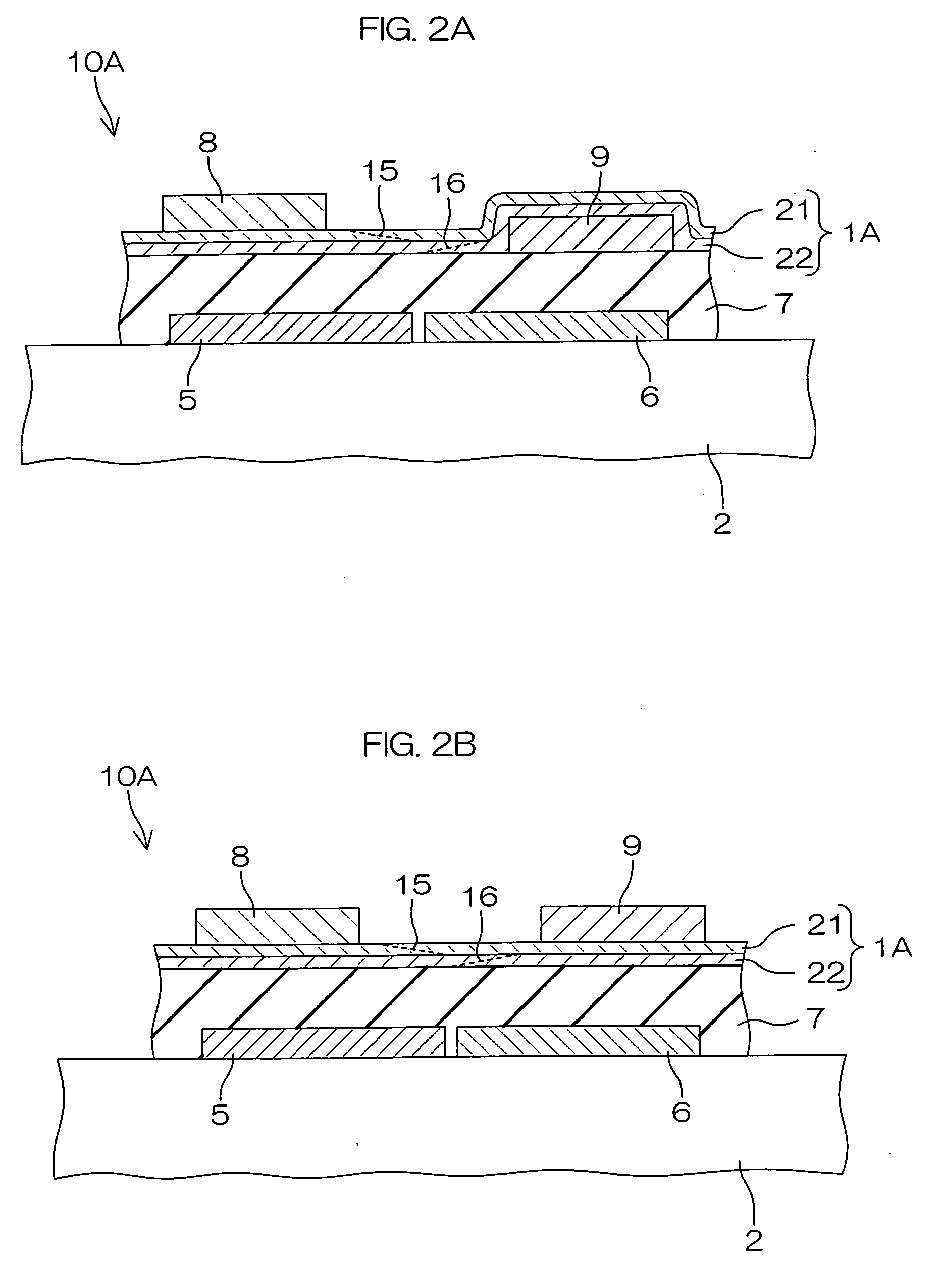
[0043]FIG. 1 is a schematic sectional view for describing an arrangement of an organic semiconductor device according to one embodiment of the present invention. The organic semiconductor device 10 is an organic light emitting element (organic electroluminescence (EL) element) that recombines electrons and holes in an organic semiconductor layer 1 (organic semiconductor light emitting layer) to emit light. The organic semiconductor 10 comprises: a hole-side gate electrode 5 and an electron-side gate electrode 6 formed as being spaced apart from each other on a substrate 2; a gate insulating film 7 (insulating layer) formed as to cover the gate electrodes 5 and 6; the organic semiconductor layer 1 laminated on the gate insulating layer 7; a hole injecting electrode 8 (hole giving / receiving electrode) and an electron injecting electrode 9 (electron giving / receiving electrode) formed apart from each other on the organic semiconductor 1. In other words, on one side of the organic semico...


PUM


Abstract

An organic semiconductor device in which recombination of holes and electrons and photoelectric conversion in an organic semiconductor layer are efficiently allowed to occur. The device comprises a bipolar organic semiconductor layer where electrons and holes move, a hole giving/receiving electrode which gives/receives holes to/from the organic semiconductor layer, an electron giving/receiving electrode which is spaced a predetermined distance from the hole giving/receiving electrode and gives/receives electrons to/from the organic semiconductor layer, a hole-side gate electrode which is opposed to a region of the organic semiconductor layer near the hole giving/receiving electrode with an insulating layer between the hole-side gate electrode and the region and serves to control the hole distribution in the organic semiconductor layer, and an electron-side gate electrode which is opposed to the region of the organic semiconductor layer with the insulating layer therebetween and serves to control the electron distribution in the organic semiconductor layer.

Description

TECHNICAL FIELD[0001]The present invention relates to an organic semiconductor device that comprises an organic semiconductor layer and a pair of electrodes that gives / receives holes and electrons to / from the organic semiconductor layer respectively, and a display and an imager using the same.BACKGROUND ART[0002]An organic EL (electroluminescence) device, a typical example of an organic semiconductor device, is a light emitting element which utilizes a luminous phenomenon during recombination of electrons and holes in an organic semiconductor layer. More specifically, the organic EL device comprises an organic semiconductor light emitting layer, an electron injecting electrode for injecting electrons to the organic semiconductor light emitting layer, and a hole injecting electrode for injecting holes to the organic semiconductor light emitting layer (refer to Japanese Unexamined Patent Publication No. 05-315078 (1993)).[0003]To improve the light emitting efficiency, the number of ca...

Claims


Application Information

Patent Timeline
Patent Type & Authority Applications(United States)
IPC IPC(8): H01L51/52H01L51/44H01L27/146H05B33/26H01L27/32H01L51/50H04N5/335H04N5/369H05B33/14
CPCH01L27/3234H01L51/5296H01L27/3244H10K59/65H10K59/12H10K50/30H05B33/14H01L27/146H10K99/00
Inventor ADACHI, CHIHAYASUGANUMA, NAOTOSHI
Owner KYOTO UNIV
Why Eureka
Try Eureka