Light emitting device

a technology of light-emitting devices and light-emitting resins, which is applied in the direction of semiconductor devices, semiconductor/solid-state device details, electrical devices, etc., can solve the problems of affecting the use, and affecting the use life, so as to prevent peeling at the interface between the reflection portion and the package, strengthen the package, and prevent the effect of peeling

Active Publication Date: 2011-07-21
NICHIA CORP
View PDF7 Cites 43 Cited by
  • Summary
  • Abstract
  • Description
  • Claims
  • Application Information

AI Technical Summary

Benefits of technology

[0010]In this regard, it is the object of the present invention to provide a light emitting device that strengthens the adhesion between the lead frame and the package, that prevents interfacial peeling between the lead frame and the package, that prevents discoloration of the package due to light from the light emitting element, and that enables efficient radiation of heat produced by the light emitting element.
[0012]A light emitting device formed with the above configuration enables light from the light emitting element to be reflected by the reflection portion that has high reflectance, and prevents discoloration of the package. Furthermore the adhesion between the reflection portion and the package is strengthened by disposing a portion of the inner wall surface of the reflection portion in an inner portion of the package. Therefore, peeling at the interface between the reflection portion and the package can be prevented.
[0014]This configuration prevents the light from the light emitting element from coming into direct contact with the opening upper side, and thereby prevents discoloration of the package.
[0020]According to the present invention, a light emitting device can be provided in which the adhesion between the reflection portion which is bent a part of the lead frame, and the package can be strengthened, and peeling at the interface of the reflection portion and the package can be prevented, furthermore, discoloration of the package caused by light from the light emitting element can be prevented, and heat produced by the light emitting element and the phosphors can be efficiently radiated.

Problems solved by technology

Such sealing resins come into contact with the lead frame, and therefore are adversely affected by the heat that is radiated by the lead frame or heat that is transmitted to the lead frame.
In other words, although the method that is disclosed in Japanese Unexamined Patent Laid-Open Application No. 2008-53726 is effective in relation to prevention of discoloration of the inner wall of the package, since the contact surface area of the sealing resin and the lead frame is large, the problem arises that the use life is shortened due to a progression of discoloration of the sealing resin due to heat transmitted in the lead frame.
Furthermore since the adhesion between the lead frame and the sealing resin is lower than that between the package and the sealing resin, there is the problem that peeling tends to occur at the interface between the lead frame and the sealing resin.

Method used


Image

  • Light emitting device
  • Light emitting device
  • Light emitting device

Examples


first embodiment

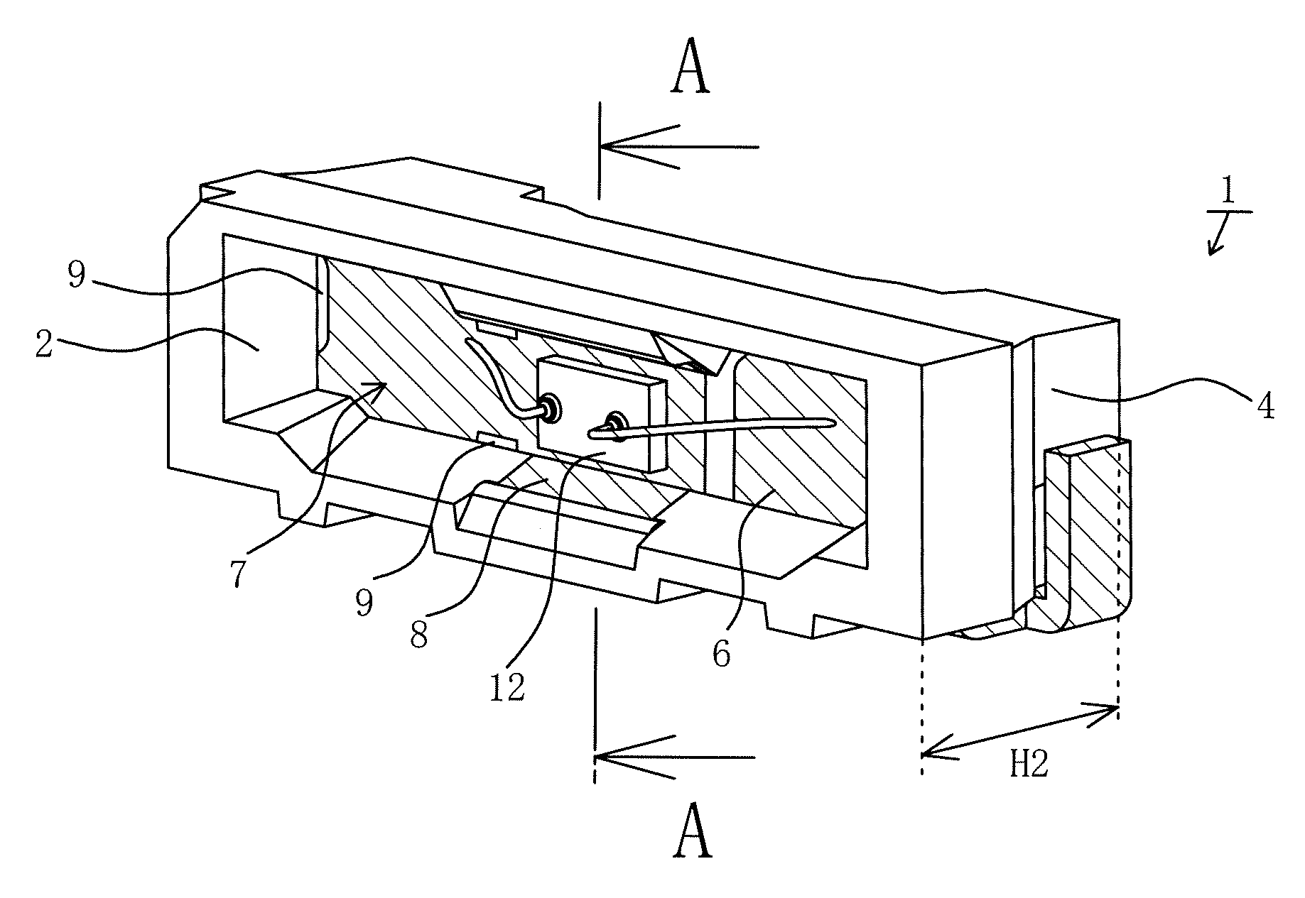
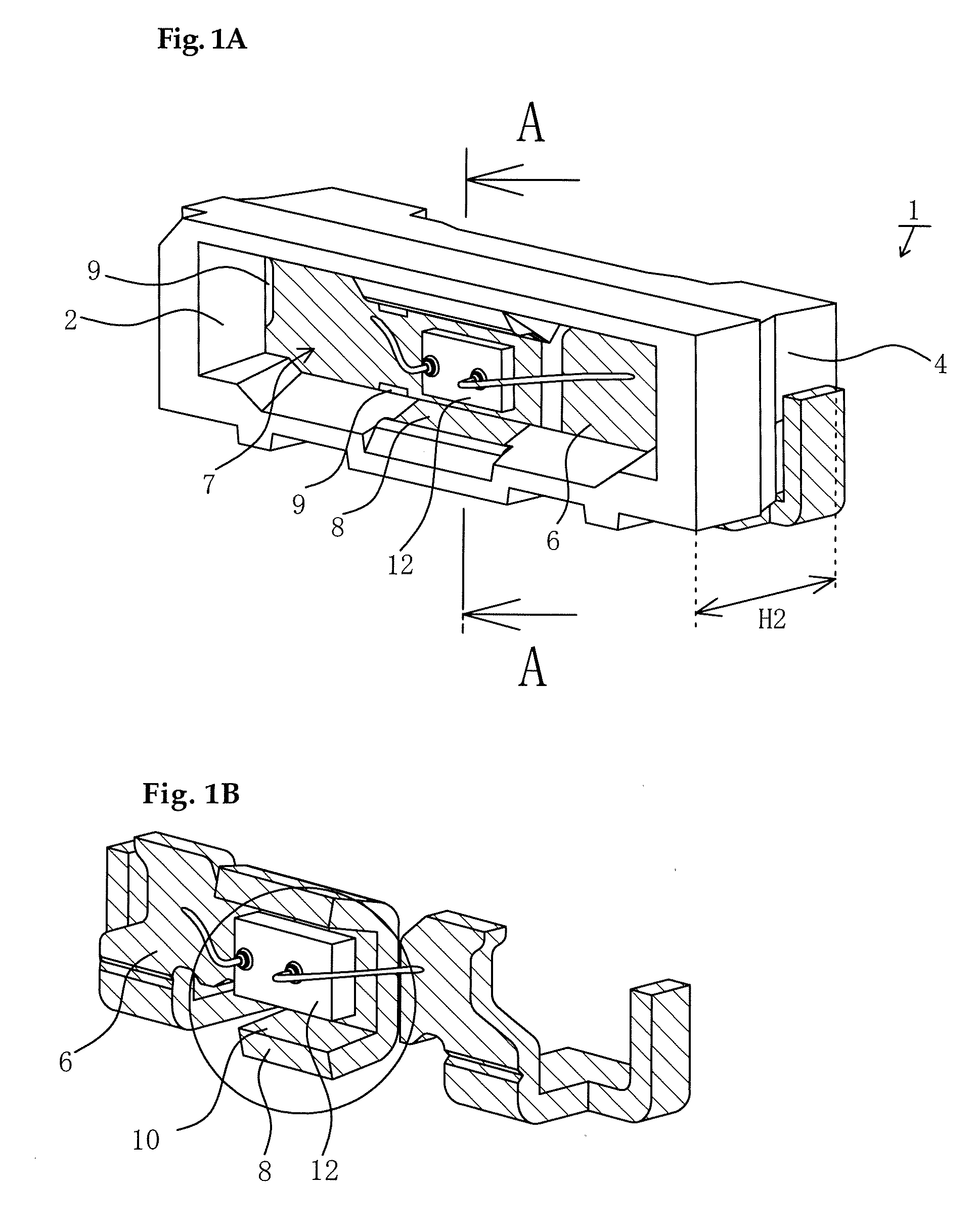
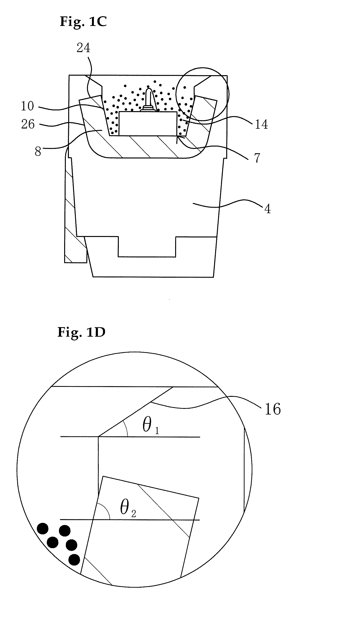
[0054]FIG. 1A is a perspective view of a light emitting device according to the present invention. FIG. 1B is a perspective view of a lead frame in the light emitting device according to the present invention. FIG. 1C is a sectional view along A-A in FIG. 1A. FIG. 1D is a partial enlarged view of FIG. 1C. FIG. 1E is a partial enlarged view of FIG. 1B. FIG. 2A is a front view showing another light emitting device according to the present invention. FIG. 2B is a back view of FIG. 2A. FIG. 2C is a plan view of FIG. 2A. FIG. 2D is a bottom view of FIG. 2A. FIG. 2E is a right side view of FIG. 2A. FIG. 2F is a left side view of FIG. 2A. FIG. 2G is a perspective view seen from an upper inclination of FIG. 2A. FIG. 2H is a perspective view seen from a rear inclination of FIG. 2A. FIG. 2I is a sectional view along A-A in FIG. 2A. FIG. 2J is a front diagonal view of the sealing member in FIG. 2A. FIG. 2K is a front view showing the state when the sealing member is not filled. FIG. 3A-FIG. 3F...

second embodiment

[0107]FIG. 5 to FIG. 10 show the external appearance of a light emitting device 100 according to a second embodiment of the present invention, and show sectional views of a lead frame 102 that can be applied to the present invention. In these figures, FIG. 5 is a front view of a light emitting device 100, FIG. 6 is a sectional perspective view along the line A-A in FIG. 5, FIG. 7 is a sectional perspective view along the line B-B in FIG. 5, FIG. 8 is a perspective view seen from an upper inclination of the side opposed to the front surface (hereinafter referred to as “back surface”), and FIG. 9 and FIG. 10 show a lead frame 102 used in a light emitting body according to the present embodiment.

[0108]The light emitting device 100 shown in these figures includes a package 101 that has a recessed portion on its front surface, a lead frame 102 exposed on the bottom surface of the recessed portion, and a light emitting element 103 that is mounted on the lead frame 102. The recessed portio...

third embodiment

[0144]The shape of the light emitting device is not limited to the above configuration, and various shapes may be used. An example is shown in FIG. 12 of a light emitting device that varies the shape of the projecting portion. FIG. 12(a) is a front view, (b) is a rear view, (c) is a plan view, (d) is a bottom view, (e) is a left view, and (f) is a right view. As shown in FIG. 12(b), the projecting portion 202b that is disposed on the back surface side of the package is formed to avoid contact with the resin injection port (gate) 108 that is used during injection molding of the package. The same effect as the second embodiment is obtained by this configuration.


PUM


Abstract

A light emitting device has a package having an opening provided with a side surface and a bottom surface, and a lead frame exposed to the bottom surface. The lead frame includes a reflection portion bent on the side surface, and a portion of an inner wall surface of the reflection portion is positioned in an inner portion of the package. A light emitting device has a package having a recessed portion on a front surface, a lead frame exposed to a bottom surface of the recessed portion, a light emitting element disposed on the lead frame, and a sealing resin filled into the recessed portion. The lead frame includes a bent portion bent towards the front surface of the package in the recessed portion, and a projecting portion bent to project from the package towards an outer portion, and disposed on a face opposed to the front surface.

Description

CROSS-REFERENCE TO RELATED APPLICATIONS[0001]This U.S. national phase application claims priority to Japanese Patent Application Nos. 2008-194918 and 2008-195484, both filed on Jul. 29, 2008, the entire disclosures of which are hereby incorporated herein by reference.TECHNICAL FIELD[0002]The present invention relates to a light emitting device using a light emitting element, and in particular relates to a thin light emitting device used as a back light or the like in a liquid-crystal display.BACKGROUND ART[0003]In recent years, high-luminance, high-output light emitting elements or small light emitting devices have been developed for use in various technical fields. These types of light emitting devices are characterized by small size, low power consumption, low weight, or the like, and for example, find application as a light source of mobile telephones and the light source of liquid-crystal back lights, the light source of various types of meters, and various types of reading sens...

Claims


Application Information

Patent Timeline
Patent Type & Authority Applications(United States)
IPC IPC(8): H01L33/50H01L33/52
CPCH01L2224/48091H01L33/62H01L2924/01322H01L2924/01019H01L33/486H01L2924/3025H01L2924/01021H01L2224/48465H01L33/60H01L2924/00014H01L2924/00
Inventor KANADA, MORITOASAKAWA, HIDEO
Owner NICHIA CORP
Why Eureka
Try Eureka