Chip package and method for forming the same

a technology of chip package and chip, applied in the direction of semiconductor/solid-state device details, electrical apparatus, semiconductor devices, etc., can solve the problems of affecting the performance of chip package, increasing fabrication cost and time,

Active Publication Date: 2011-08-11
XINTEC INC
View PDF39 Cites 39 Cited by
  • Summary
  • Abstract
  • Description
  • Claims
  • Application Information

AI Technical Summary

Benefits of technology

[0009]According to an embodiment of the invention, a chip package is provided, which includes: a substrate having an upper surface and a lower surface; a hole extending from the upper surface toward the lower surface; an insulating layer located overlying a sidewal

Problems solved by technology

However, the formed conducting layer may suffer from problems such as cracking or high stress at a bottom corner in the hole, such that the performance of the chip package is affected.
In addition, in the conventional chip packaging technique, a complex patterning process needs to be applied, such that a plurality of photoresist applica

Method used


Image

  • Chip package and method for forming the same
  • Chip package and method for forming the same
  • Chip package and method for forming the same

Examples


Embodiment Construction

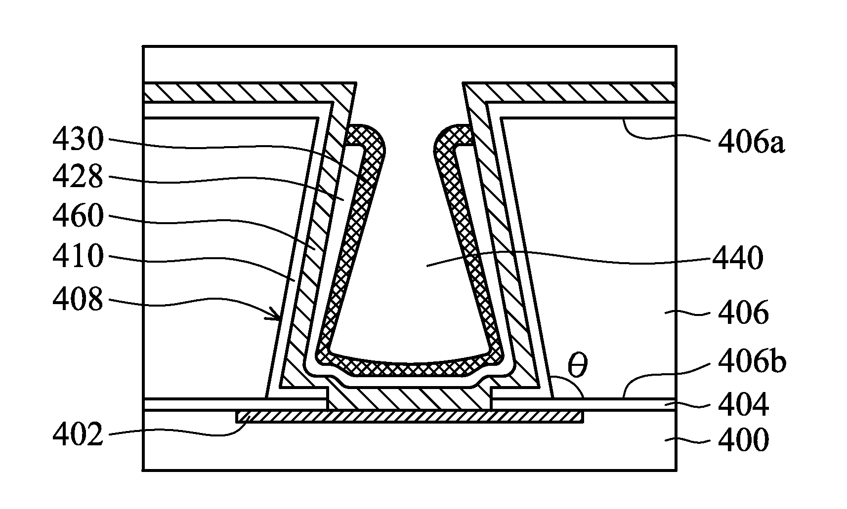
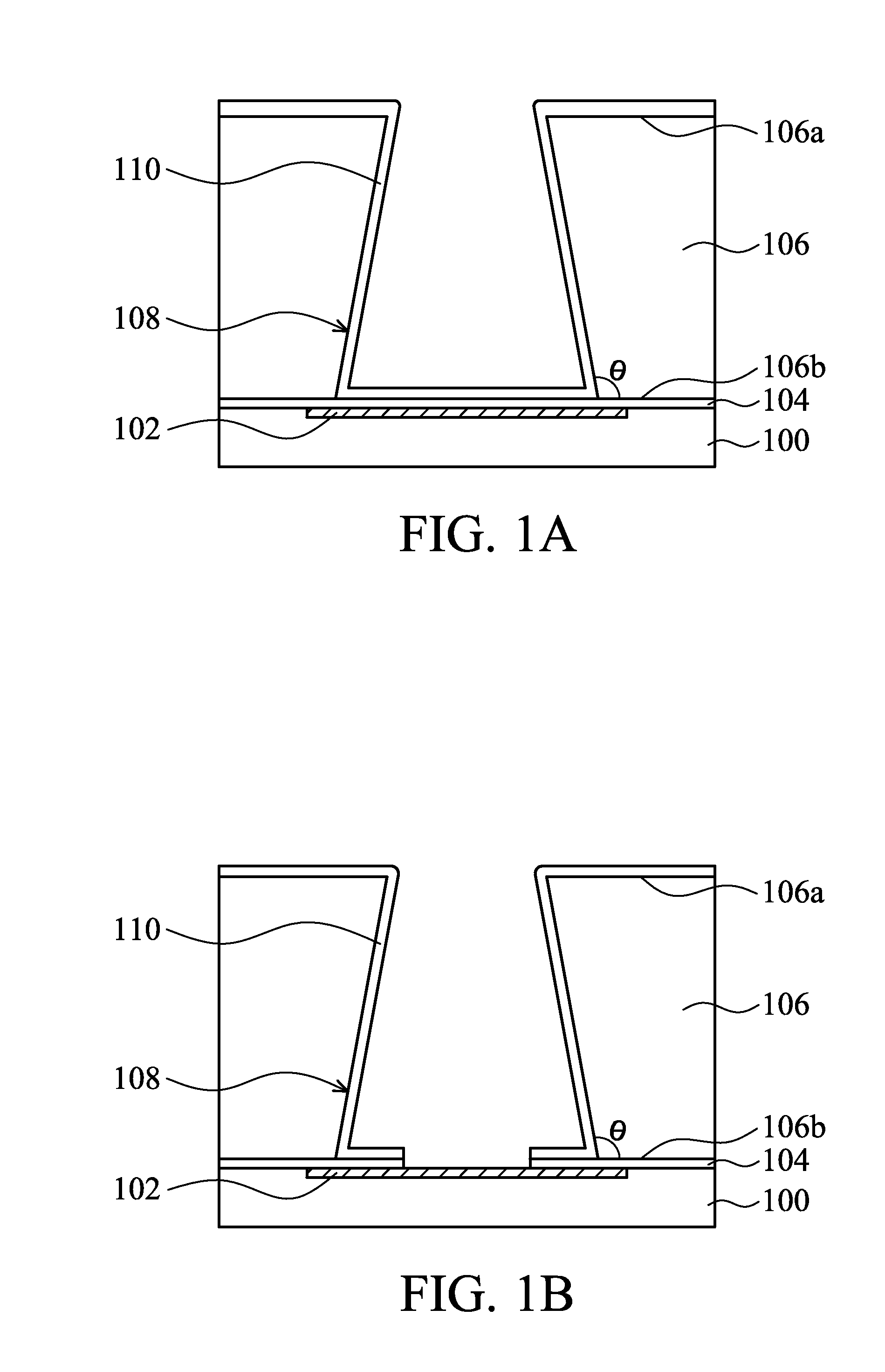
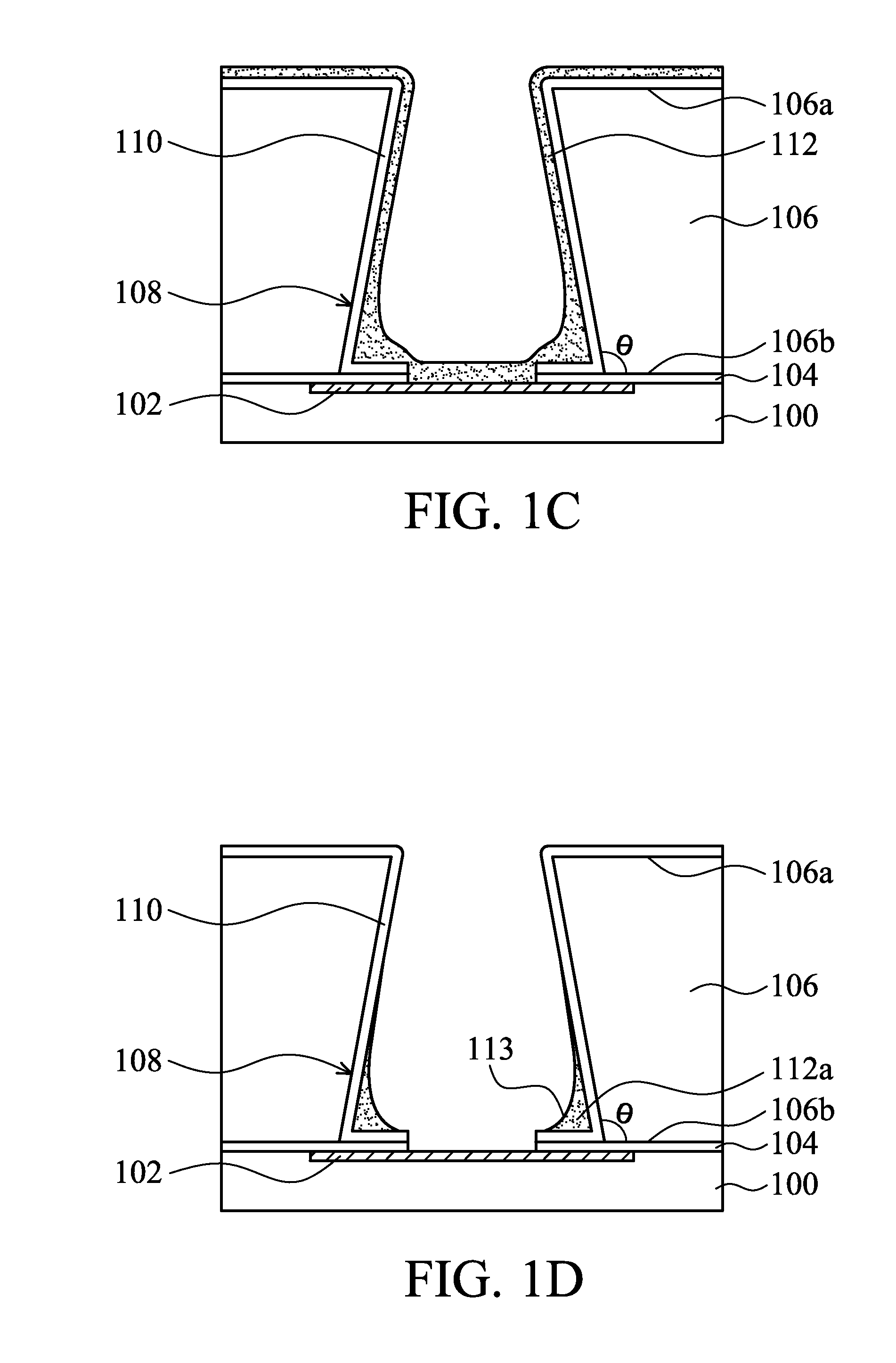
[0017]The following description is of the best-contemplated mode of carrying out the invention. This description is made for the purpose of illustrating the general principles of the invention and should not be taken in a limiting sense. The scope of the invention is best determined by reference to the appended claims.

[0018]It is understood, that the following disclosure provides many different embodiments, or examples, for implementing different features of the invention. Specific examples of components and arrangements are described below to simplify the present disclosure. These are, of course, merely examples and are not intended to be limiting. In addition, the present disclosure may repeat reference numbers and / or letters in the various examples. This repetition is for the purpose of simplicity and clarity and does not in itself dictate a relationship between the various embodiments and / or configurations discussed. Furthermore, descriptions of a first layer “on,”“overlying,” (...


PUM


Abstract

According to an embodiment of the invention, a chip package is provided, which includes: a substrate having an upper surface and a lower surface; a hole extending from the upper surface toward the lower surface; an insulating layer located overlying a sidewall of the hole; and a material layer located overlying the sidewall of the hole, wherein the material layer is separated from the upper surface of the substrate by a distance and a thickness of the material layer decreases along a direction toward the lower surface.

Description

CROSS REFERENCE TO RELATED APPLICATIONS[0001]This Application claims the benefit of U.S. Provisional Application No. 61 / 302,848, filed on Feb. 9, 2010, the entirety of which is incorporated by reference herein. This Application claims the benefit of U.S. Provisional Application No. 61 / 331,642, filed on May 5, 2010, the entirety of which is incorporated by reference herein.BACKGROUND OF THE INVENTION[0002]1. Field of the Invention[0003]The present invention relates to a chip package and formation method thereof, and in particular relates to a chip package having a through substrate hole and formation method thereof.[0004]2. Description of the Related Art[0005]Recently, conducting structures (such as TSVs) perpendicular to a surface of a package substrate are commonly being formed in chip packages to form a conducting path along a vertical direction. As a result, space may be employed more effectively, such that the size of the chip package is further shrunk, which helps to improve pe...

Claims


Application Information

Patent Timeline
IPC IPC(8): H01L23/48H01L21/768
CPCH01L21/76898H01L23/481H01L24/05H01L2224/0557H01L2924/01078H01L2924/01079H01L2924/14H01L2924/0002H01L2924/1461H01L2924/00H01L2224/05552H01L21/486H01L21/76804H01L21/76877H01L2224/0501H01L23/49827
Inventor YEN, YU-LINYANG, MING-KUNLIU, TSANG-YUYEOU, LONG-SHENG
Owner XINTEC INC
Why Eureka
Try Eureka