

Liquid crystal display panel
- Summary
- Abstract
- Description
- Claims
- Application Information
AI Technical Summary
Benefits of technology
Problems solved by technology
Method used
Image

Examples
Embodiment Construction
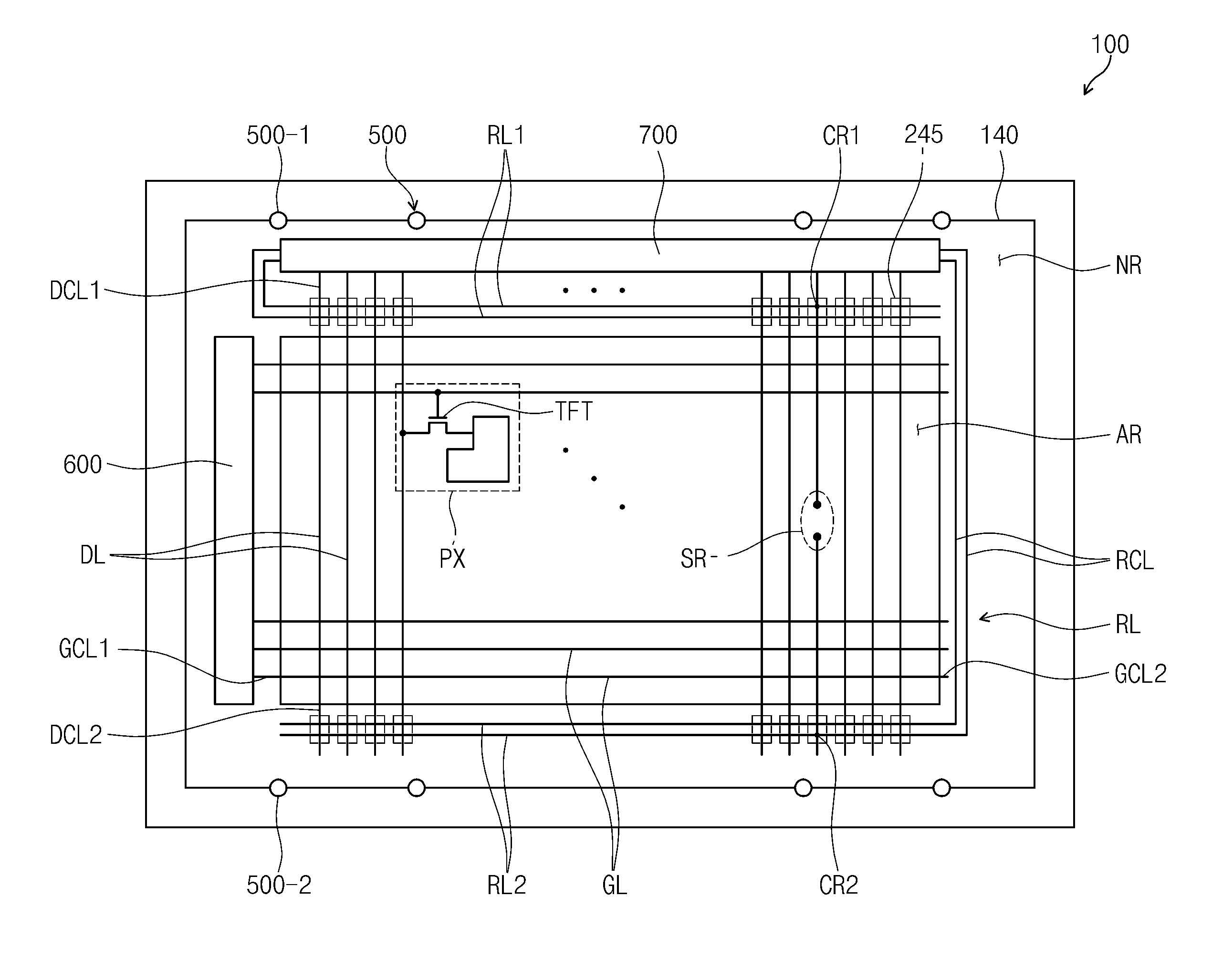
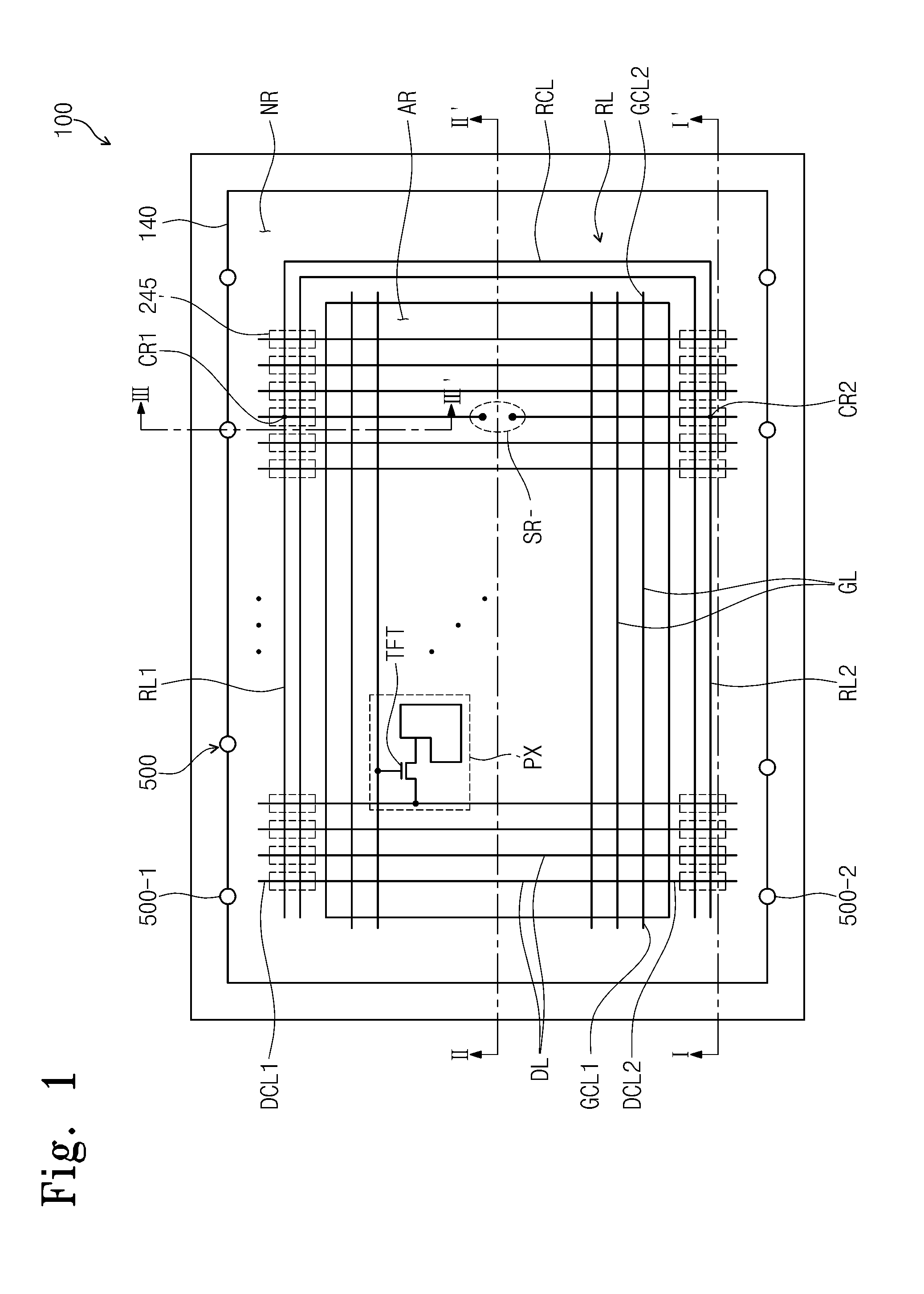
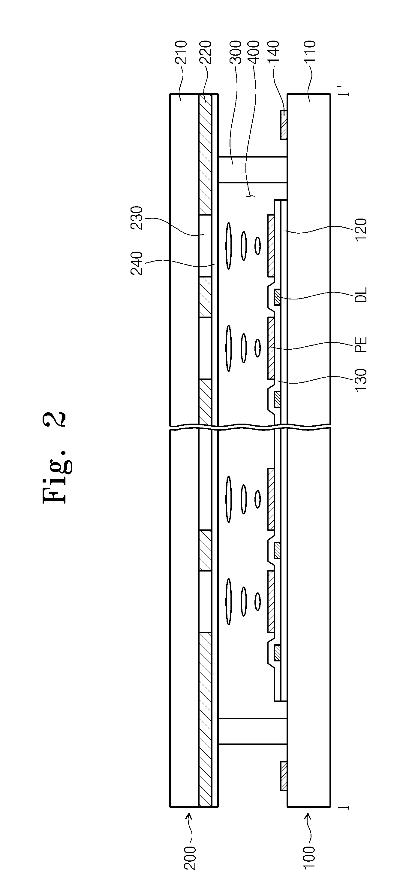
[0026]The present invention can be modified in various forms and may not be limited to the following embodiments but include various applications and modifications. The following embodiments are provided to clarify the technical spirit disclosed in the present invention and to sufficiently transmit the technical spirit of the present invention to a person of ordinary skill in this field. Therefore, the scope of the present invention should not be limited to the following embodiments. For example, although the examples provided are in the context of liquid crystal display panels, the invention may be adapted to other types of display panels.
[0027]When describing each attached drawing, similar reference numerals are designated as similar components. In addition, the size of the layers and regions of the attached drawings along with the following embodiments are simplified or exaggerated for precise explanation or emphasis and the same reference numeral represents the same component. T...
PUM
 Abstract
Description
Claims
Application Information