Display device

a technology of a display device and a display screen, which is applied in the direction of semiconductor devices, basic electric elements, electrical appliances, etc., can solve the problems that the semiconductor layer (also referred to as the active layer) of the transistor may be damaged

Pending Publication Date: 2022-05-05
SAMSUNG DISPLAY CO LTD
View PDF3 Cites 0 Cited by
  • Summary
  • Abstract
  • Description
  • Claims
  • Application Information

AI Technical Summary

Problems solved by technology

A semiconductor layer (also referred to as an active layer) constituting a transistor may be damaged when the display device is deformed due to a high modulus of elasticity.

Method used


Image

  • Display device
  • Display device
  • Display device

Examples


Embodiment Construction

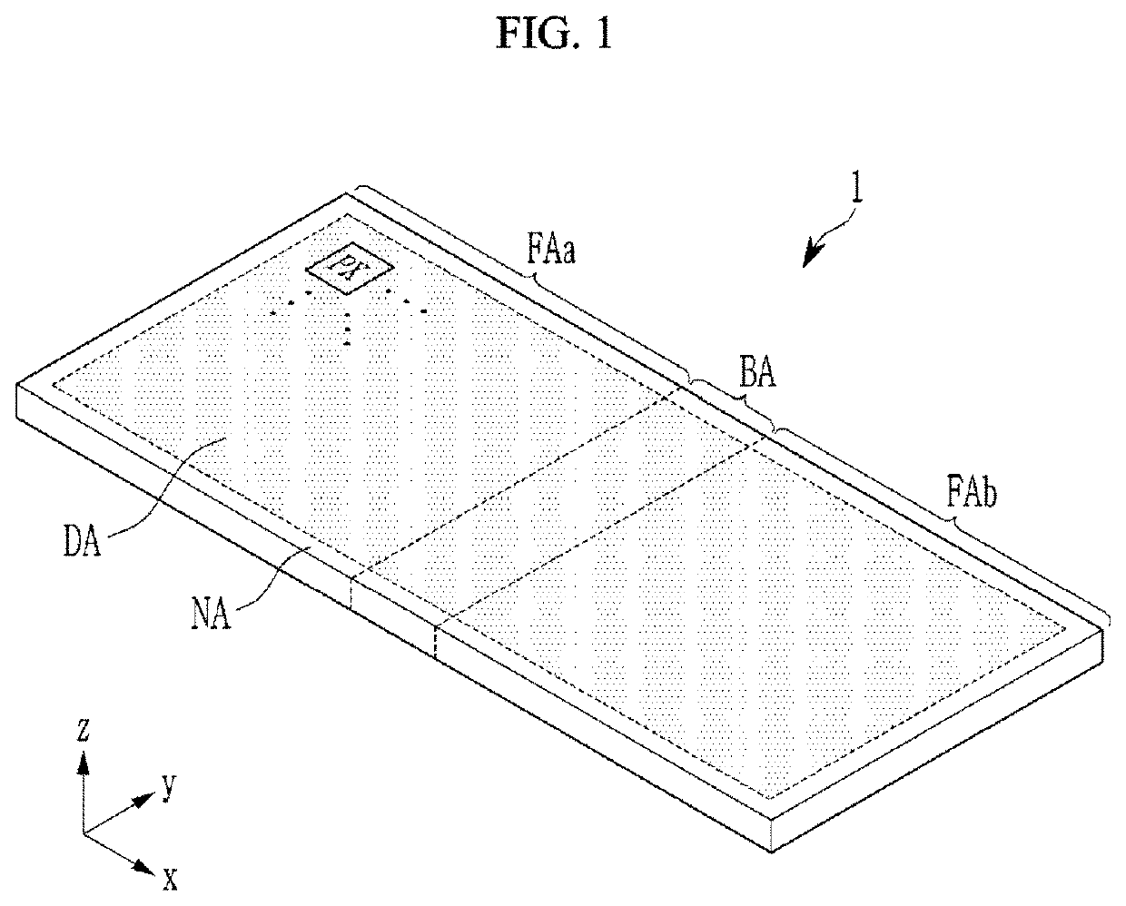
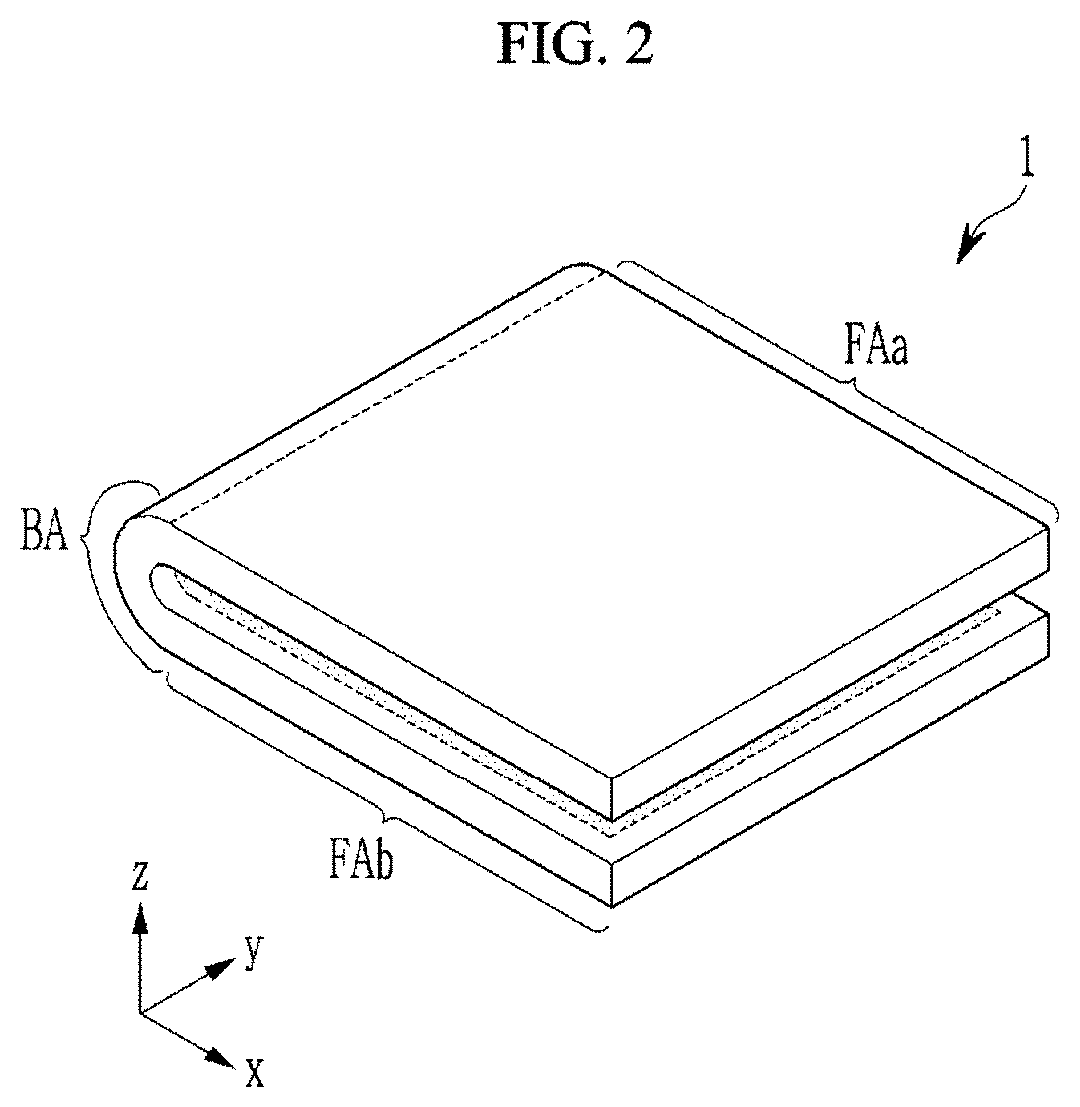
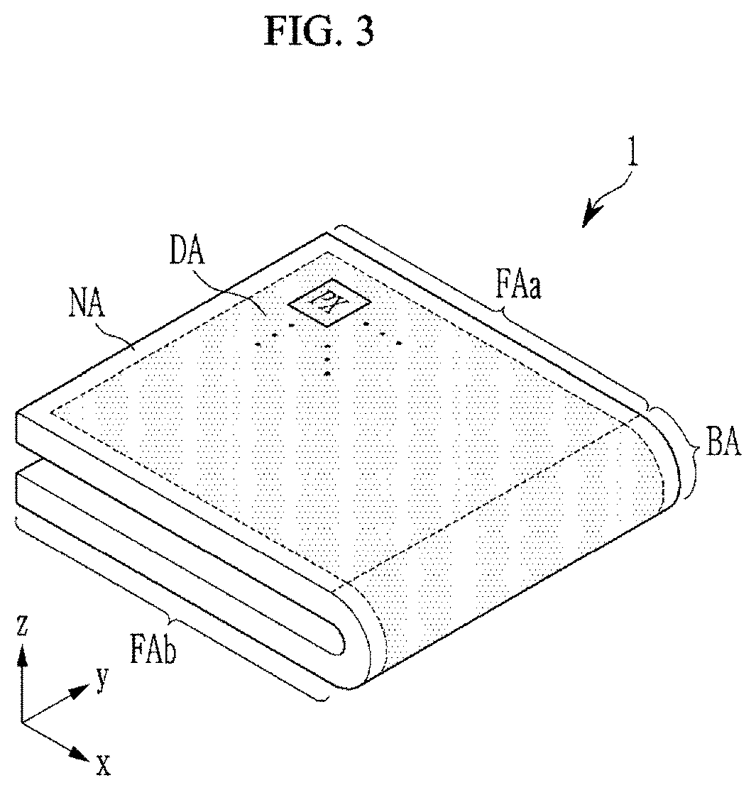
[0038]The present disclosure will be described more fully hereinafter with reference to the accompanying drawings, in which embodiments are shown.

[0039]Further, sizes and thicknesses of constituent elements shown in the accompanying drawings are arbitrarily given for better understanding and ease of description.

[0040]It will be understood that when an element such as a layer, film, area, or substrate is referred to as being “on” another element, it can be directly on the other element or intervening elements may also be present. In contrast, when an element is referred to as being “directly on” another element, there are no intervening elements present.

[0041]In addition, unless explicitly described to the contrary, the word “comprise” and variations such as “comprises” or “comprising” will be understood to imply the inclusion of stated elements but not the exclusion of any other elements.

[0042]In addition, in the specification, “connected” means that two or more components are not o...


PUM

PropertyMeasurementUnit
structuresaaaaaaaaaa
thicknessaaaaaaaaaa
mechanical reliabilityaaaaaaaaaa

Abstract

A display device includes a substrate and a transistor disposed on the substrate and including a semiconductor layer, wherein the semiconductor layer includes a mesh structure, and wherein a plurality of openings are formed in the semiconductor layer.

Description

CROSS-REFERENCE TO RELATED APPLICATION[0001]This application claims priority to and benefits of Korean Patent Application No. 10-2020-0143366, filed in the Korean Intellectual Property Office on Oct. 30, 2020, the entire contents of which are incorporated herein by reference.BACKGROUND(a) Technical Field[0002]The present disclosure relates to a display device. More particularly, the present disclosure relates to a display device capable of securing mechanical reliability even when the display device is deformed.(b) Description of the Related Art[0003]Electronic devices such as mobile phones, tablets, multimedia players, and televisions include display devices for displaying images. Each of the display devices includes a display panel that implements a screen displaying an image. A flexible display device capable of deformation such as bending, folding, rolling, and stretching by using a flexible substrate as a substrate for a display panel has been developed.[0004]The above informat...

Claims


Application Information

Patent Timeline
Patent Type & Authority Applications(United States)
IPC IPC(8): H01L27/12
CPCH01L27/1222H01L27/3262H01L27/1225H01L27/1218H10K59/88H10K59/1213H10K10/484H10K77/111H10K2102/311H01L27/1237H01L27/124H10K59/124H10K50/00
Inventor LEE, WOO BINBANG, SEOK HWANSON, SEUNG SOKLEE, WOO GEUNCHAE, SOO JUNG
Owner SAMSUNG DISPLAY CO LTD
Why Eureka
Try Eureka