Multi-domain liquid crystal display device with particular dielectric structures

a liquid crystal display and dielectric structure technology, applied in non-linear optics, instruments, optics, etc., can solve the problems of weak electric field distortion needed to divide the pixel region, and decrease in brightness

Inactive Publication Date: 2005-05-31
LG DISPLAY CO LTD
View PDF45 Cites 74 Cited by
  • Summary
  • Abstract
  • Description
  • Claims
  • Application Information

AI Technical Summary

Benefits of technology

[0017]The dielectric frame maintains uniformly gap between the first and second

Problems solved by technology

If the electrodes do not have an open area or the width of the open area is narrow, the electric field distortion needed to divide the pixel region becomes weak.
At this ti

Method used


Image

  • Multi-domain liquid crystal display device with particular dielectric structures
  • Multi-domain liquid crystal display device with particular dielectric structures
  • Multi-domain liquid crystal display device with particular dielectric structures

Examples


Embodiment Construction

[0036]Hereinafter, the multi-domain liquid crystal display device of the present invention is explained in detail by accompanying the drawings.

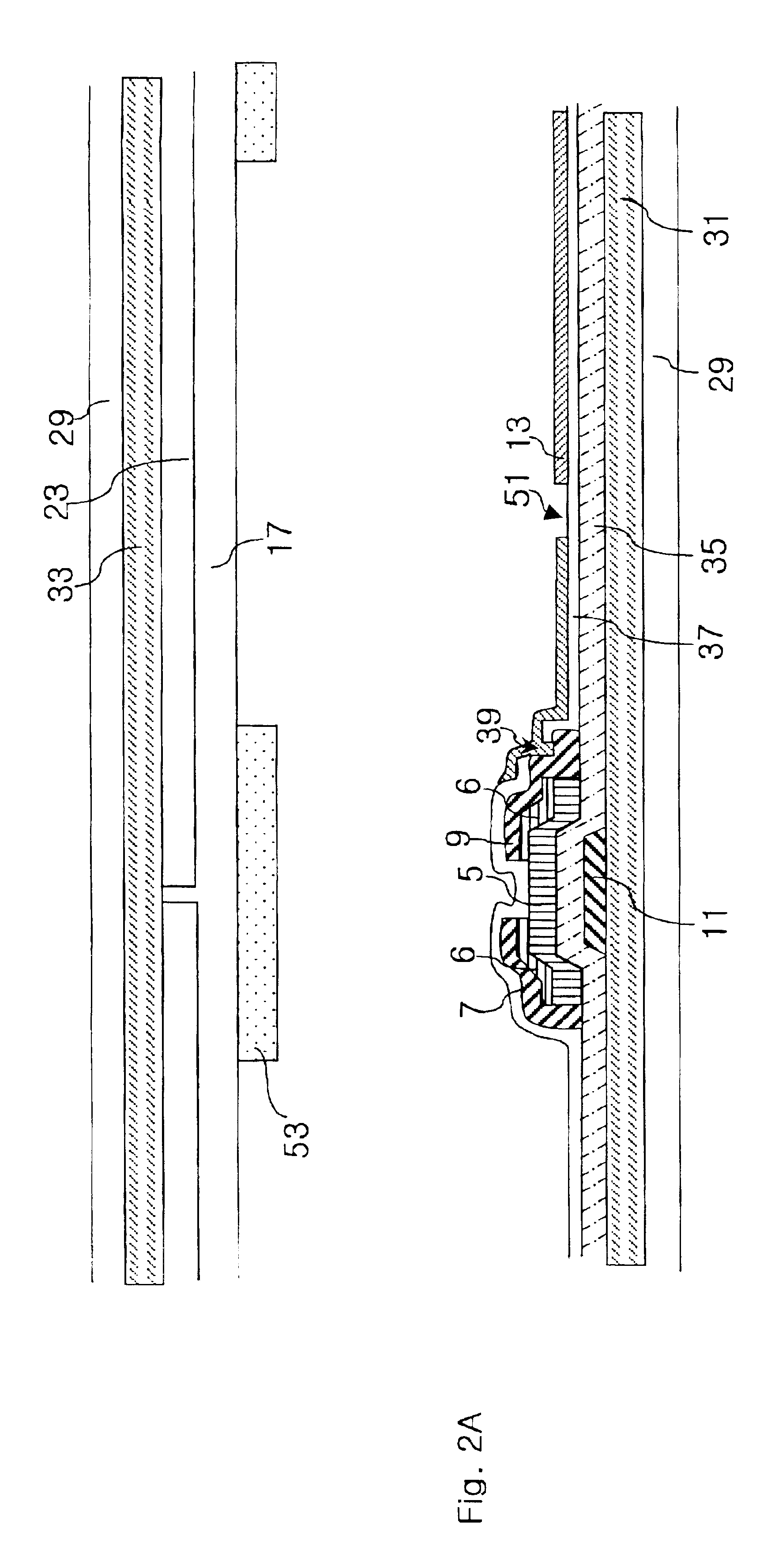
[0037]FIGS. 2A, 2B, 2C, and 2D are sectional views of the multi-domain liquid crystal display devices according to the first embodiment of the present invention and FIGS. 3A, 3B, and 3C are sectional views of the multi-domain liquid crystal display devices according to the second embodiment of the present invention.

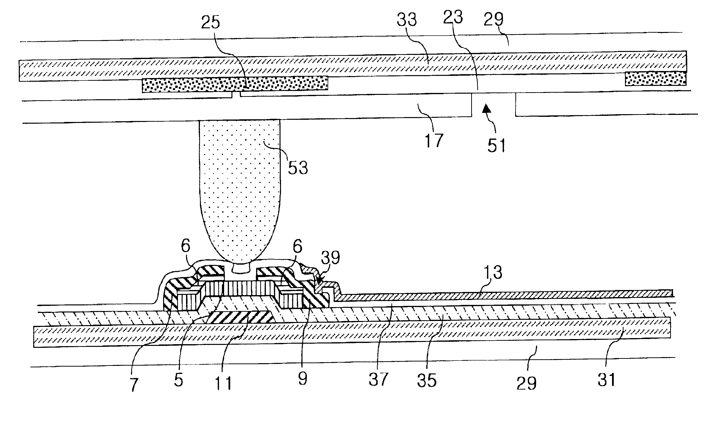
[0038]As shown in the figures, the present invention comprises first and second substrates 31, 33, a plurality of gate bus lines 1 arranged in a first direction on a first substrate and a plurality of data bus lines 3 arranged in a second direction on the first substrate, a TFT, a passivation layer 37, and a pixel electrode 13.

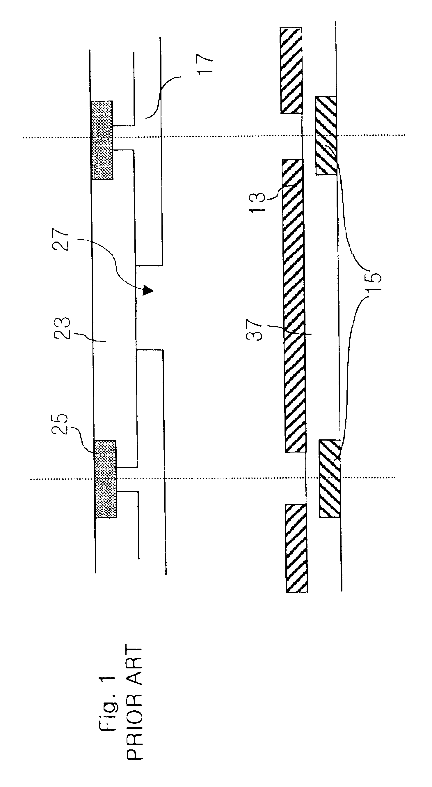
[0039]On the second substrate 33, a light shielding layer 25 is formed to shield the light leaked from gate and data bus lines 1, 3, and the TFT, a color filter layer 23 is formed on the light shielding layer...


PUM


Abstract

A multi-domain liquid crystal display device includes first and second substrates facing each other and a liquid crystal layer between the first and second substrates. A plurality of gate bus lines are arranged in a first direction on the first substrate and a plurality of data bus lines are arranged in a second direction on the first substrate to define a pixel region. A pixel electrode is electrically charged through the data bus line in the pixel region. A dielectric frame is in a region other than a region where the pixel electrode is formed, and distorts electric field applied to the liquid crystal layer. A common electrode is on the second substrate, and an alignment layer is on at least one substrate between the first and second substrates.

Description

[0001]This application claims the benefit of Korean Application No. 1998-50708 filed Nov. 25, 1998 and No. 1999-05401 filed Feb. 18, 1999, which are hereby incorporated by reference. This application also incorporates by reference U.S. patent application Ser. No. 09 / 326,415 filed Jun. 4, 1999, entitled “MULTI-DOMAIN LIQUID CRYSTAL DISPLAY DEVICE” and Ser. No. 09 / 421,114 filed Oct. 19, 1999, entitled “A MULTI-DOMAIN LIQUID CRYSTAL DISPLAY DEVICE,” both of which are assigned to the same assignee as the present application.BACKGROUND OF THE INVENTION[0002]1. Field of the Invention[0003]The present invention relates to a liquid crystal display device (LCD), and more particularly, to a liquid crystal display device having a dielectric frame.[0004]2. Description of the Related Art[0005]Recently, an LCD has been proposed where the liquid crystal is not aligned and the liquid crystal is driven by common-auxiliary electrodes insulated from pixel electrodes. FIG. 1 is sectional view of pixel ...

Claims


Application Information

Patent Timeline
IPC IPC(8): G02F1/13G02F1/1333G02F1/1335G02F1/1337G02F1/139
CPCG02F1/133707G02F1/133512G02F1/1393G02F1/133753
Inventor LEE, YUN BOKKIM, KYEONG JINYOO, JANG JINLEE, JAE YOONKWON, DO HEE
Owner LG DISPLAY CO LTD
Why Eureka
Try Eureka