Light emitting diode

a light-emitting diode and wavelength conversion technology, which is applied in the direction of basic electric elements, electrical equipment, semiconductor devices, etc., can solve the problems of troublesome work, high cost, limited size of the above-mentioned surface-mounted type led, etc., and achieves simple structure and easy and inexpensive mounting.

Inactive Publication Date: 2008-03-18
CITIZEN ELECTRONICS CO LTD
View PDF5 Cites 8 Cited by
  • Summary
  • Abstract
  • Description
  • Claims
  • Application Information

AI Technical Summary

Benefits of technology

[0015]An object of the present invention is to provide an LED capable of easy and inexpensive mounting by a simple structure and flexible to design changes, in particular, thickness, of a case of an electronics device such as a mobile phone using LED, when the LED is used as an electric flash light source used in the electronics device.
[0017]Another object of the present invention is to provide an LED which prevents separation of a substrate and a translucent sealing resin at a surface boundary thereof by eliminating a reflow process, and having high reliability and stability for a long period.

Problems solved by technology

However, a size of the above-mentioned surface mount type LED is limited by the design of a belonging electronics device, in particular, the thickness, of a case of an electronics device in which the LED is mounted.
Accordingly, there is a problem that this results in troublesome work and very high cost.
In addition, because a process in which an LED is heated in the reflow device and mounted on a mother board of an electronics device by soldering is required for a surface mount type LED, there is a problem that the LED element itself and other parts used for the LED need to be heat resistant.
Furthermore, when the LED passes through the reflow process, there is a problem that separation of the substrate and the translucent sealing resin at the surface boundary thereof and disconnection of the bonding wires occur easily, thereby reducing reliability, stability, and so on.

Method used


Image

  • Light emitting diode
  • Light emitting diode
  • Light emitting diode

Examples


first embodiment

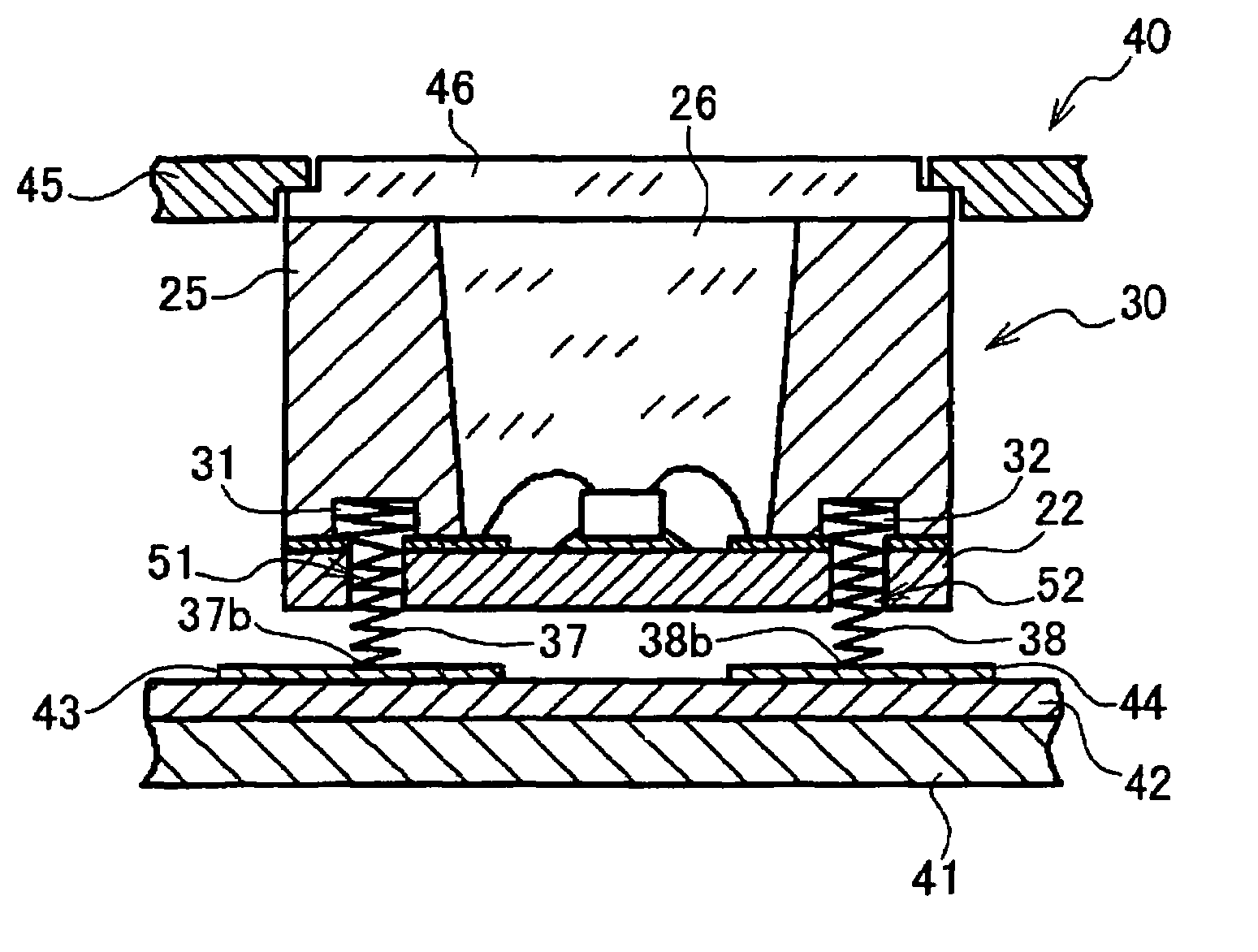
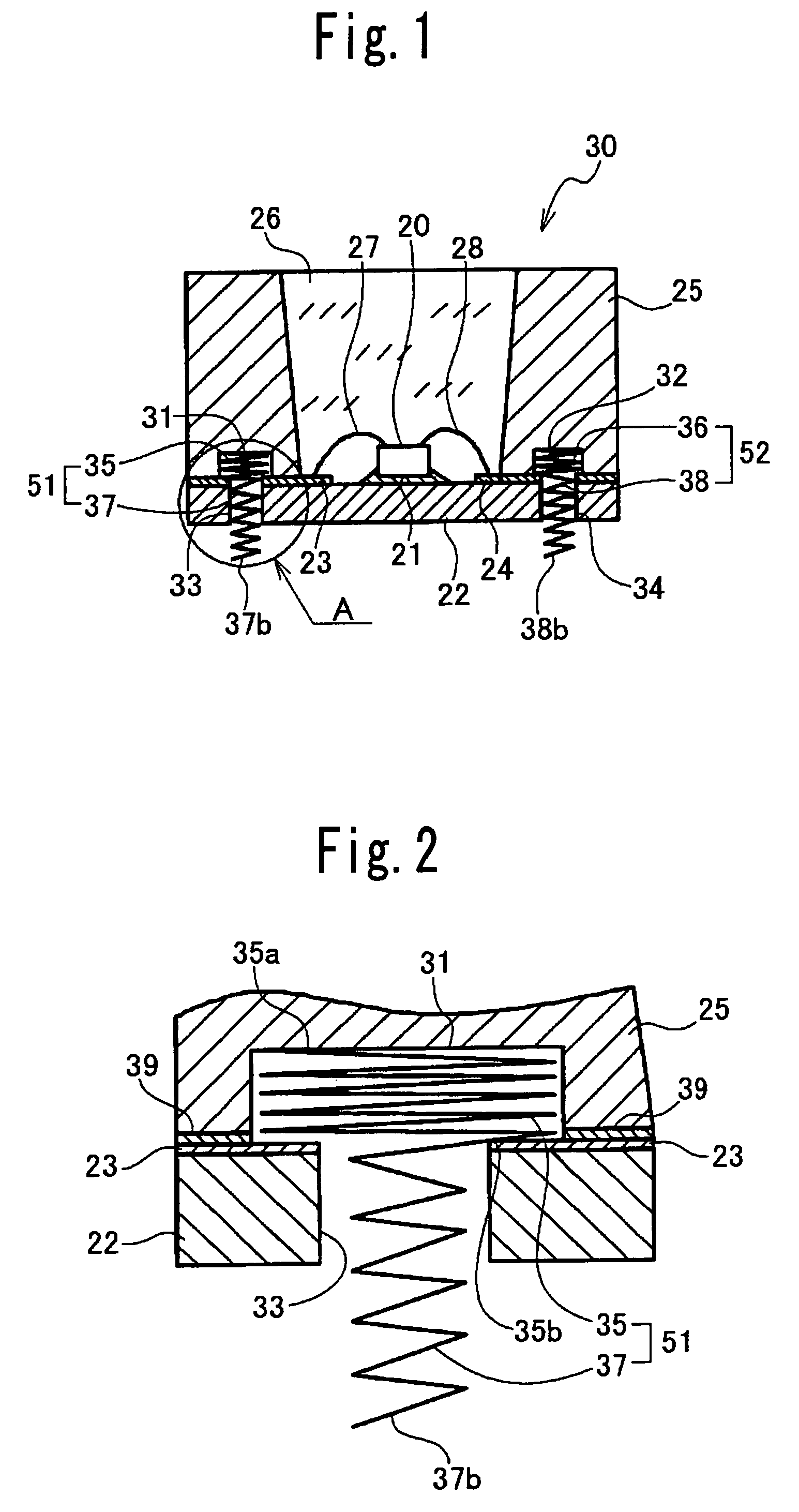
[0045]an LED according to the present invention is shown in FIGS. 1 to 5.

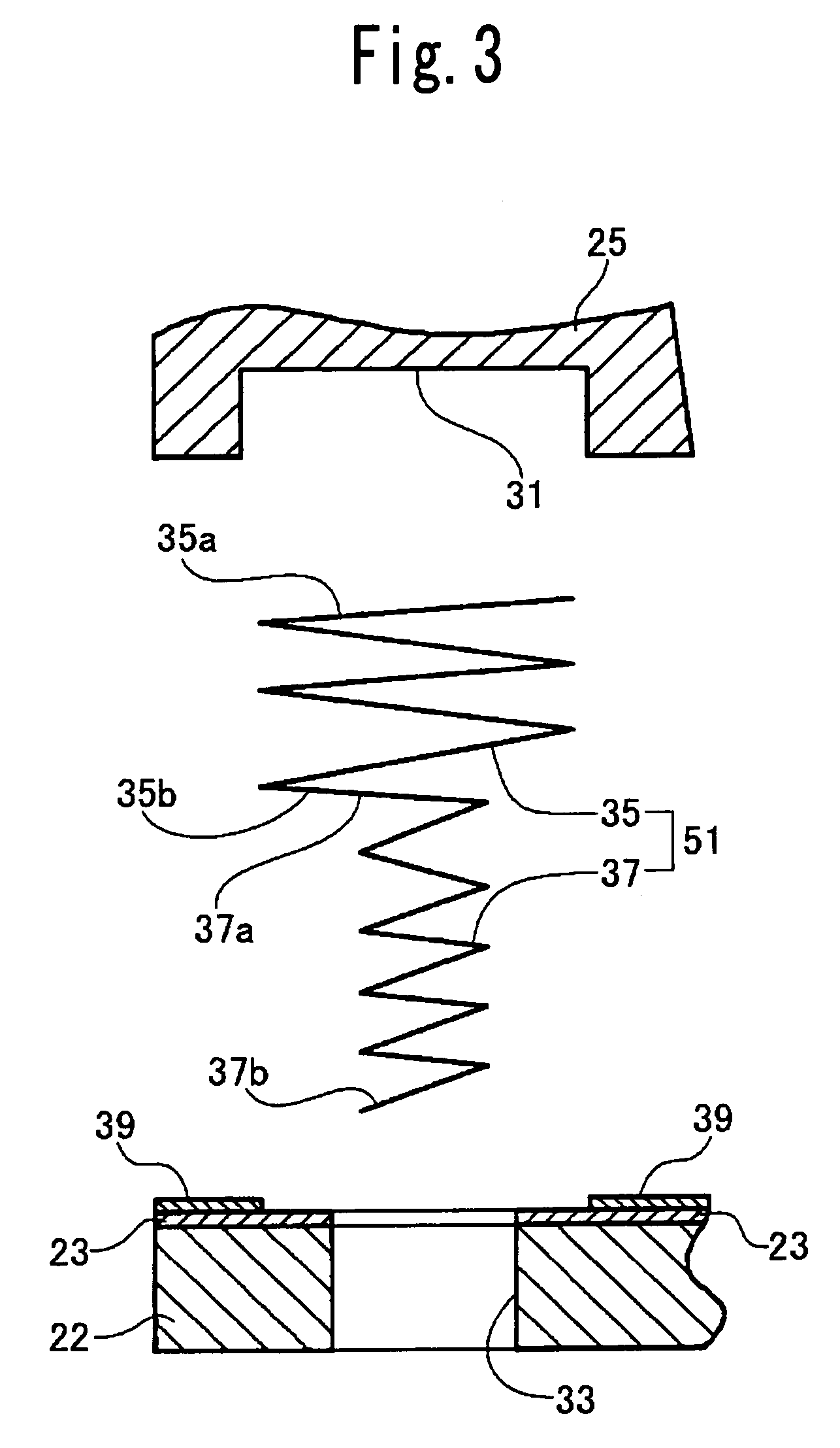
[0046]The LED 30 in the first embodiment includes a substrate 22 and a pair of terminal electrodes provided on the substrate 22, as shown in FIG. 1. The substrate 22 is made of a rectangular glass epoxy resin and has an upper surface and a lower surface. In a case that a plurality of LEDs are manufactured in an aggregation, the substrate is preferably square-shaped. The terminal electrodes are patterned on the upper surface of the substrate 22 and include a cathode electrode 23 and an anode electrode 24.

[0047]The cathode and anode electrodes 23 and 24 are made of gold, silver, or copper to which aluminum plating is applied, or the like.

[0048]At least one LED element 20 is mounted on and fixed to a central portion of the upper surface of the substrate 22 through a fluorescent material-containing layer 21. Of course, the fluorescent material and a dye may be contained in a translucent sealing resin and the number...


PUM


Abstract

An LED including a substrate having a pair of terminal electrodes, at least one LED element mounted on the substrate, a frame disposed on the substrate, holes provided in the substrate, concave portions provided in positions of the frame facing the holes, and a pair of conductive elastic members provided between the frame and the substrate, each of the conductive elastic members including a large diameter portion inserted in the corresponding concave portion and a small diameter portion inserted in the corresponding hole and electrically connected to the large diameter portion, the large diameter portions of the pair of conductive elastic members being electrically connected to the pair of terminal electrodes, respectively, and each of the large diameter portions having one end portion which is in contact with a bottom surface of the concave portion and each of the small diameter portions having one end portion which is disposed to project from the hole of the substrate.

Description

CROSS-REFERENCE TO THE RELATED APPLICATION[0001]This application is based on and claims the priority benefit of Japanese Patent Application No. 2005-25682 filed on Feb. 1, 2005, the contents of which are incorporated herein by reference in their entirety.BACKGROUND OF THE INVENTION[0002]1. Field of the Invention[0003]The present invention relates to a wavelength-conversion type light emitting diode (LED), more specifically to a white LED used to illuminate a subject when photographing the subject with a camera which is installed in an electronics device such as a mobile phone.[0004]2. Description of Related Art[0005]Recently, there has been an accelerated multifunctionization of mobile electronics devices such as mobile phones; in particular, mobile phones in which digital cameras are installed have become widely used. Furthermore, mobile phones including an electric flash structure for outputting flash light for photography have been proposed (see, for reference, Japanese Patent La...

Claims


Application Information

Patent Timeline
Patent Type & Authority Patents(United States)
IPC IPC(8): H01L31/0203H01L33/62
CPCH01L33/62H01L33/486H01L2224/48091H01L2224/48227H01L2224/73265H01L2924/0102H01L2924/01068H01L2924/01079H01L2924/3025H01L2924/01078H01L2924/12041H01L2224/32225H01L2924/00014H01L2924/00H01L2924/00012H01L24/73
Inventor KIKUCHI, SATORU
Owner CITIZEN ELECTRONICS CO LTD
Why Eureka
Try Eureka