Touch panel and input device including the same

a technology of input device and touch panel, which is applied in the direction of instruments, computing, electric digital data processing, etc., can solve the problems of reducing transparency, disturbing the user's view of the display, and reducing the newton's ring, etc., and achieves the effect of simple construction

US7714845B2Inactive Publication Date: 2010-05-11PANASONIC CORP
10 Cites 9 Cited by

Patent Information

Authority / Receiving Office
US · United States
Patent Type
Patents(United States)
Current Assignee / Owner
Publication Date
2010-05-11
Estimated Expiration
Not applicable · inactive patent

Smart Images

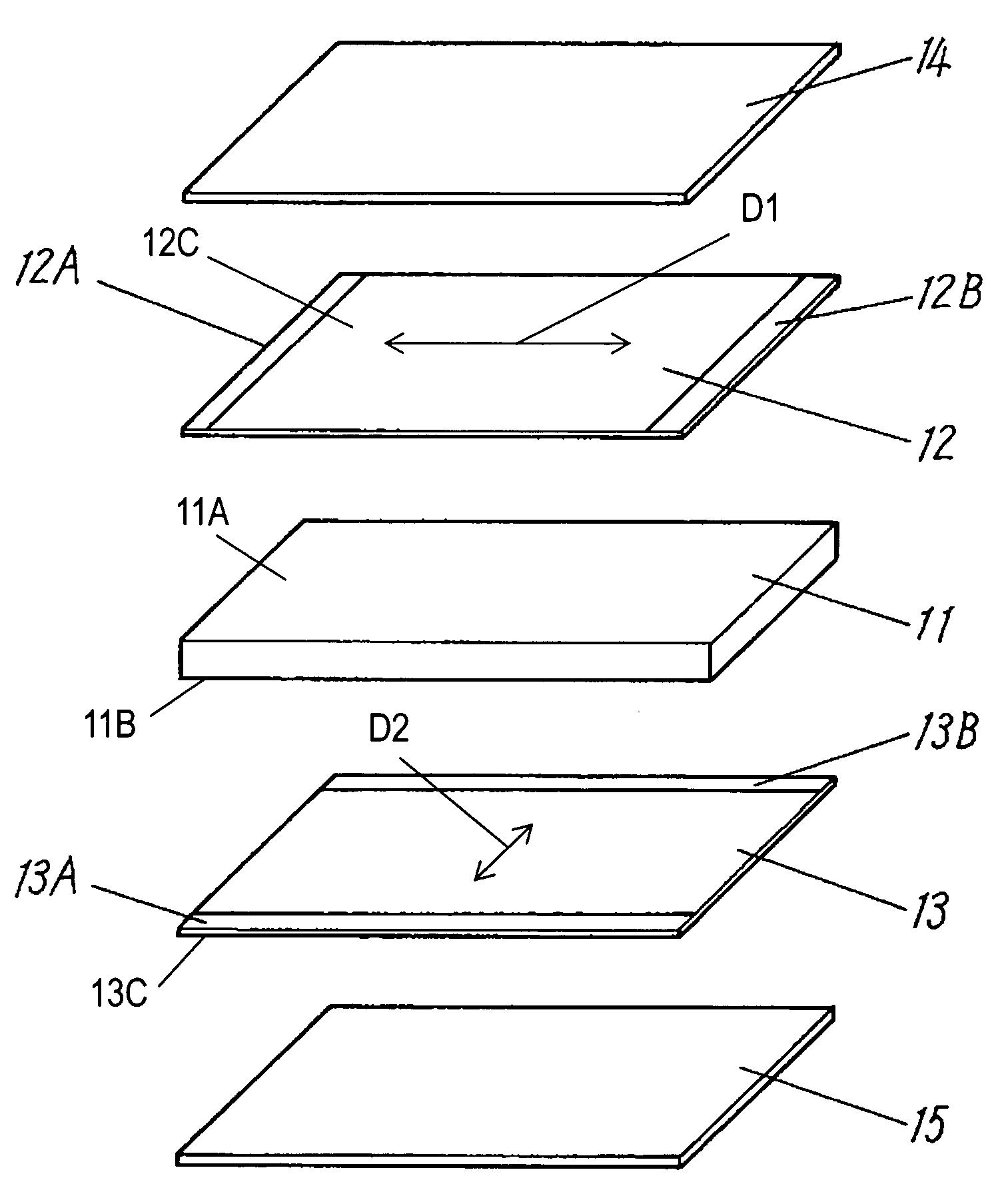
  • Figure 1
    Figure 1
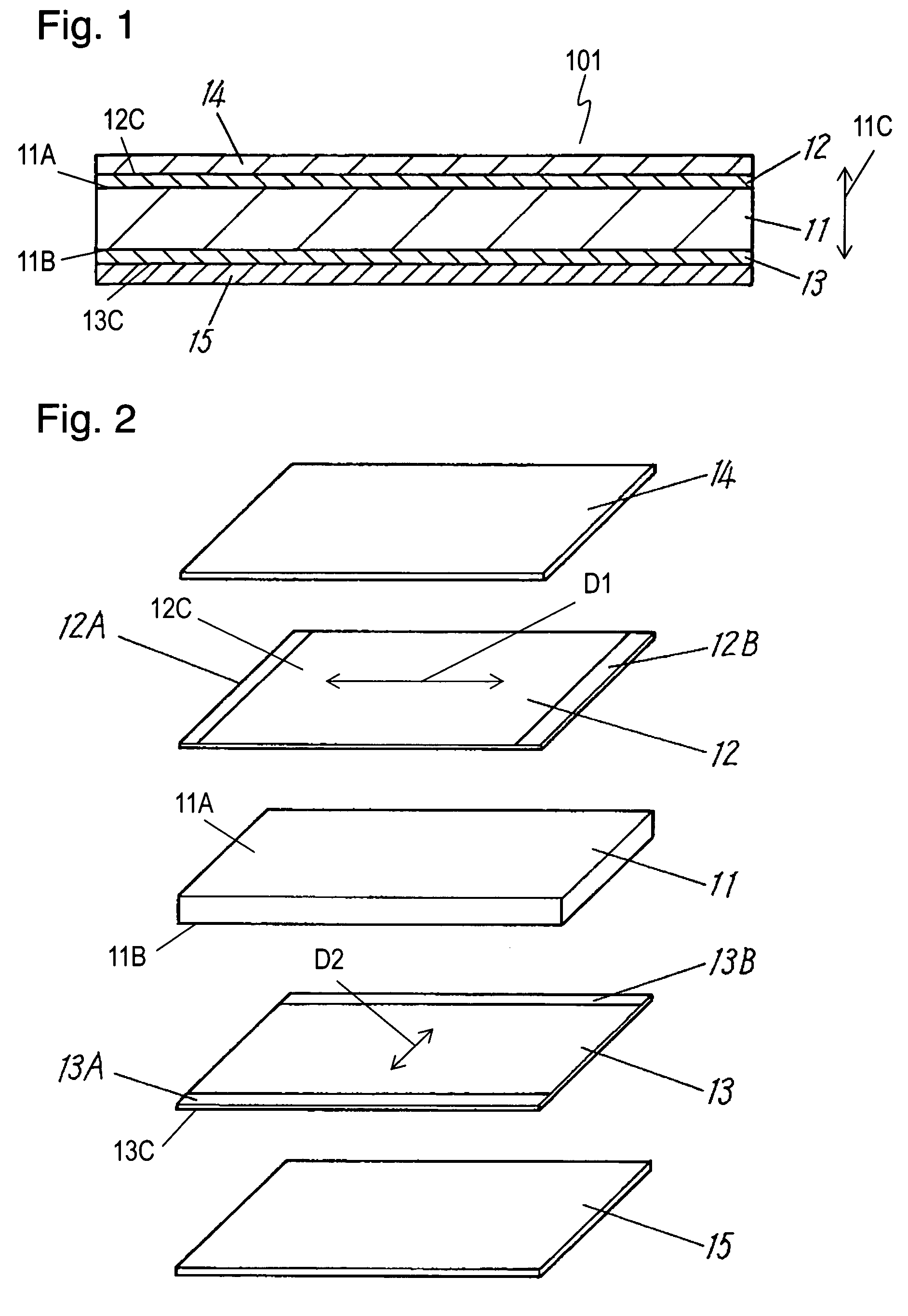
  • Figure 2
    Figure 2
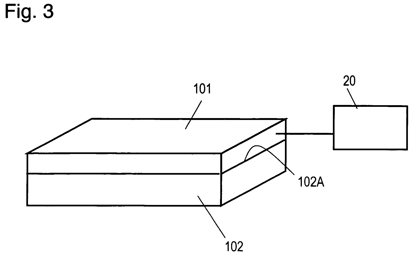
  • Figure 3
    Figure 3
Patent Text Reader

Abstract

A touch panel includes a light-transmissible, piezoelectric substrate having a first surface and a second surface opposite to the first surface of the piezoelectric substrate, a first light transmissible, resistor layer provided on the first surface of the substrate, and a second light transmissible, resistor layer provided on the second surface of the substrate. A portion of the piezoelectric substrate, upon being pressed, has an electric resistance locally decreasing. The touch panel, even having a simple construction, can avoid reflections of external light and suppress a Newton's ring.
Need to check novelty before this filing date? Find Prior Art

Description

FIELD OF THE INVENTION

[0001] The present invention relates to a touch panel used for inputting data to an electronic apparatus, and to an input device including the touch panel.BACKGROUND OF THE INVENTION

[0002] As electronic apparatuses have had multi-functions, the apparatuses employ light-transmissible touch panels mounted on screens of displays, such as liquid crystal displays, of the apparatuses. A touch panel is simply manipulated by a user to allow him / her to view and select a character, an icon, and a symbol displayed on the screen with a finger or a dedicated pen for activating desired functions.

[0003] A conventional touch panel disclosed in Japanese Patent Laid-Open Publication No. 7-169367 will be explained. FIG. 5 is a cross sectional view of the conventional touch panel. A light transmissible upper resistor layer 3 made of, for example, indium tin oxide is provided on the lower surface of an upper substrate 1 made of light transmissible film. Similarly, a light transmissibl...

Examples

Embodiment Construction

[0015]FIG. 1 is a cross sectional view of a touch panel 101 according to an exemplary embodiment of the present invention. FIG. 2 is an exploded perspective view of the touch panel 101. An upper resistor layer 12 made of light transmissible material, such as indium tin oxide or tin oxide, is formed by, for example, vacuum sputtering on the upper surface 11A of a light-transmissible, piezoelectric substrate 11 made of piezoelectric material, such as poly-vinylidene fluoride, and has a thickness ranging from 150 μm to 200 μm. A lower resistor layer 13 made of light-transmissible material, such as indium tin oxide or tin oxide, is deposited on the lower surface 11B of the substrate 11 by, for example, vacuum sputtering. The upper resistor layer 12 has an upper surface 12C coated with a hard coat layer 14 made of transparent insulating resin, such as acrylic resin, polyester resin, or epoxy resin. The lower resistor layer 13 has a lower surface 13C coated with an insulating layer 15 mad...