Check patentability & draft patents in minutes with Patsnap Eureka AI!

Display device and manufacturing method thereof

a technology of display device and manufacturing method, which is applied in the direction of semiconductor devices, instruments, electrical devices, etc., can solve the problems of deteriorating display quality of display device, loss of source electrode film or drain electrode film proportion, and reducing yield of display devi

Active Publication Date: 2013-11-19
JAPAN DISPLAY INC +1
View PDF24 Cites 0 Cited by
  • Summary
  • Abstract
  • Description
  • Claims
  • Application Information

AI Technical Summary

Benefits of technology

This method effectively prevents electrode film loss during pixel electrode formation, enhancing display quality and increasing manufacturing yield by ensuring accurate and complete electrode formation.

Problems solved by technology

However, in the manufacturing method of a display device having the Lite structure, it was found that when the pixel electrodes are formed in predetermined regions in contact with a part of the source electrode film, a problem arises that a portion of the formed source electrode film or drain electrode film is lost.
Due to the loss of a portion of the source electrode film or the drain electrode film, the display quality of the display device is deteriorated, and consequently, the yield thereof is decreased.

Method used


Image

  • Display device and manufacturing method thereof
  • Display device and manufacturing method thereof
  • Display device and manufacturing method thereof

Examples


Embodiment Construction

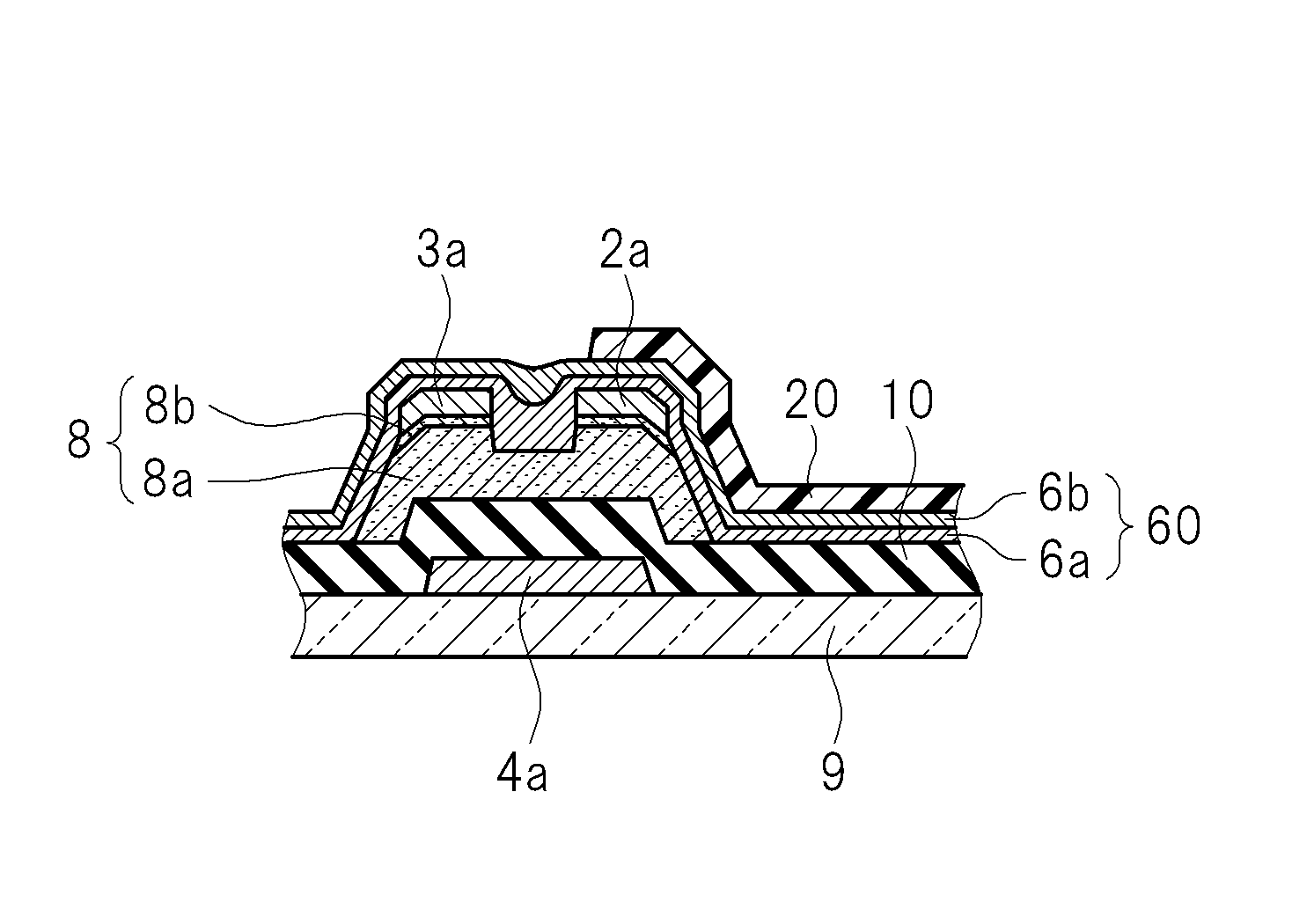
[0038]A display device manufactured by a manufacturing method of a display device according to the invention includes: a gate electrode film; a first electrode film and a second electrode film, both of which are disposed separated from the gate electrode film by an insulating film; and a conductive film which is composed of a conductive layer including a first conductive layer formed in contact with the upper surface of the first electrode film and a second conductive layer formed overlapping the first conductive layer and is formed in predetermined regions.

[0039]Further, the gate electrode film according to the invention is composed of agate electrode and a gate electrode line. Further, the first electrode film is composed of a first electrode and a first electrode line electrically connected to the first electrode. Further, the second electrode film is composed of a second electrode and a second electrode line electrically connected to the second electrode.

[0040]The manufacturing ...


PUM

PropertyMeasurementUnit
conductiveaaaaaaaaaa
transparent conductiveaaaaaaaaaa
transparentaaaaaaaaaa

Abstract

A manufacturing method of a display device including a gate electrode film, a first electrode film, a second electrode film, and a conductive film connected to the first electrode film and formed of a conductive layer including a first conductive layer and a second conductive layer formed overlapping the first conductive layer. The method includes the steps of forming the first electrode film and the second electrode film, forming the conductive layer such that the conductive layer is connected to the first electrode film and the second electrode film, and forming the conductive film by removing regions other than predetermined regions of the conductive layer, wherein the conductive layer forming step includes the steps of forming the first conductive layer on the respective upper surfaces of the first electrode film and the second electrode film and forming the second conductive layer on the upper surface of the first conductive layer.

Description

CROSS-REFERENCE TO RELATED APPLICATION[0001]The present application claims priority from Japanese patent application JP2010-006989 filed on Jan. 15, 2010, the content of which is hereby incorporated by reference into this application.BACKGROUND OF THE INVENTION[0002]1. Field of the Invention[0003]The present invention relates to a display device and a manufacturing method thereof.[0004]2. Description of the Related Art[0005]Recently, various types of display devices have been developed due to a demand for a reduction in thickness and an increase in definition of a display device. For example, an in-plane switching (IPS) mode liquid crystal display device is known as the display device.[0006]FIG. 8 is a cross-sectional view showing one example of a pixel region provided in a conventional IPS mode liquid crystal display device. As shown in FIG. 8, in order to meet the demand for a reduction in thickness and an increase in definition of a display device, the structure of the convention...

Claims


Application Information

Patent Timeline
Patent Type & Authority Patents(United States)
IPC IPC(8): H01L21/00G02F1/1343H01L31/00H01L29/04H01L21/44H01L29/10
CPCG02F1/133615G02F1/1343G02F1/136
Inventor GOTOH, JUNHATAKEYAMA, EISUKEANJO, KENJIOGISHIMA, YOSHITOMO
Owner JAPAN DISPLAY INC
Features
  • R&D
  • Intellectual Property
  • Life Sciences
  • Materials
  • Tech Scout
  • Unparalleled Data Quality
  • Higher Quality Content
  • 60% Fewer Hallucinations
Learn More