Light emitting diode element

a diode element and light-emitting technology, applied in the field of light-emitting diode elements, can solve the problems of inconvenient and short-circuit dies, ineffective solution of inconvenience and shortages, and limited light extraction efficiency of conventional led dies, so as to improve the light scattering effect, improve the whole light output quality, and increase the light extraction efficiency

Active Publication Date: 2014-05-20
LEXTAR ELECTRONICS CORP
View PDF9 Cites 4 Cited by
  • Summary
  • Abstract
  • Description
  • Claims
  • Application Information

AI Technical Summary

Benefits of technology

[0008]The present invention provides a light emitting diode element for effectively increasing the light extraction efficiency and enhancing the whole light output quality,
[0009]The present invention provides a light emitting diode element which utilizes a transversal epitaxy growth mechanism for enhancing the whole crystals to regularly grow and effectively improving the crystal quality of epitaxy.

Problems solved by technology

However, confined to the structure of the conventional LED die, the light extraction efficiency of conventional LED die is still limited, and a solution for effectively providing higher light extraction efficiency is yet to be seen.
As what is disclosed above, the conventional LED die still has inconvenience and shortages, thereby requiring an improvement.
As such, how to effectively solve the mentioned inconvenience and shortages shall be a serious issue to be concerned.
1. With the installation of the nano-spheres, the light emitting diode element of the present invention can provide a better light scattering effect, thereby increasing the light extraction efficiency and enhancing the whole light output quality.
2. The nano-spheres disposed in the buffer layer of the light emitting diode element of the present invention are closer to the light emitting structure, thereby increasing the light extraction efficiency in a more effective manner.
3. With the installation of the nano-spheres, a transversal epitaxy growth mechanism is formed in the light emitting diode element of the present invention, thereby enhancing the whole crystals to regularly grow, lowering the possibilities of generating crystal defect, and effectively improving the crystal quality of epitaxy.
4. With the nano-spheres being received in the grooves, air gaps are inevitably formed, thereby altering the light reflection rate and increasing the light scattering effect.

Method used


Image

  • Light emitting diode element
  • Light emitting diode element
  • Light emitting diode element

Examples


first embodiment

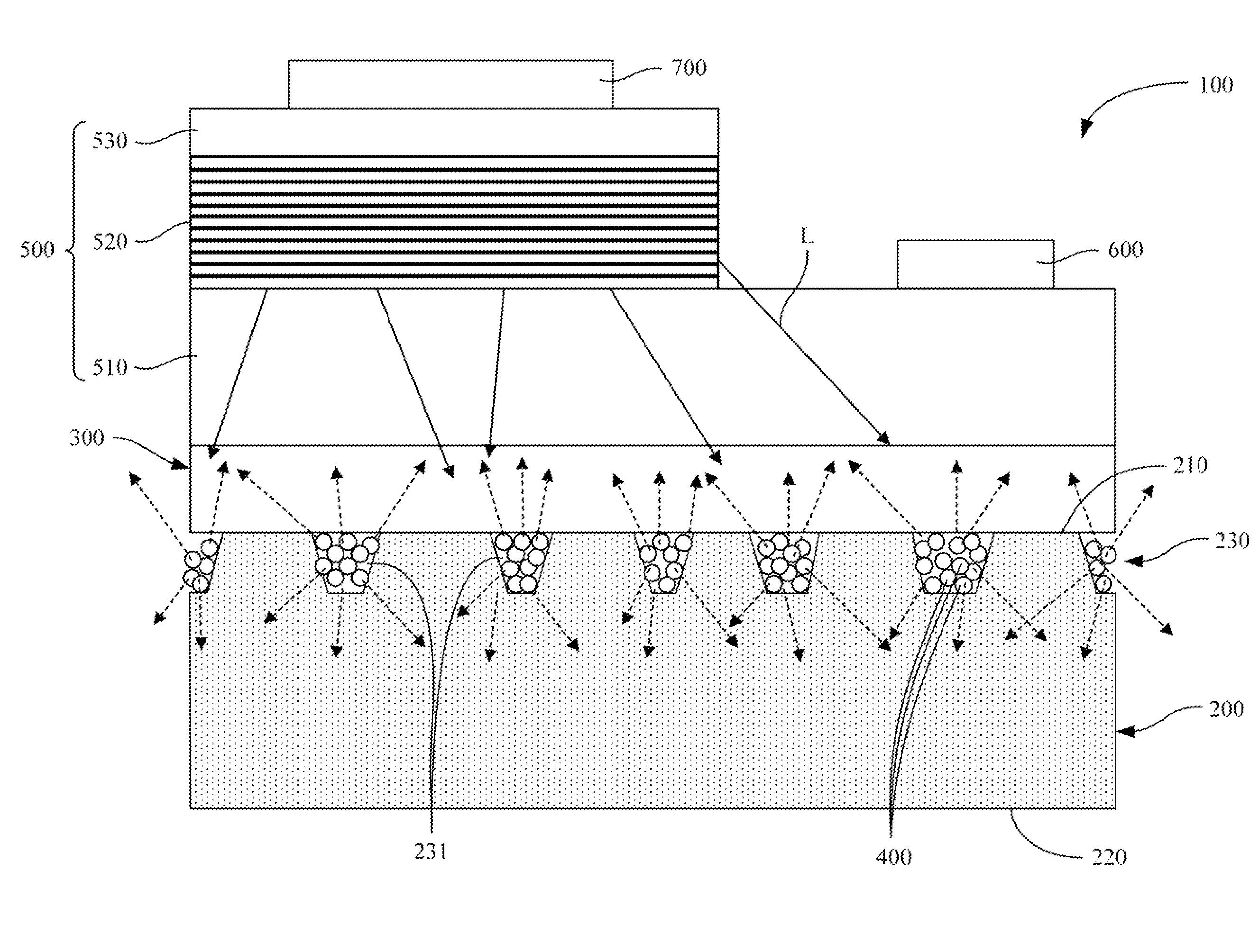
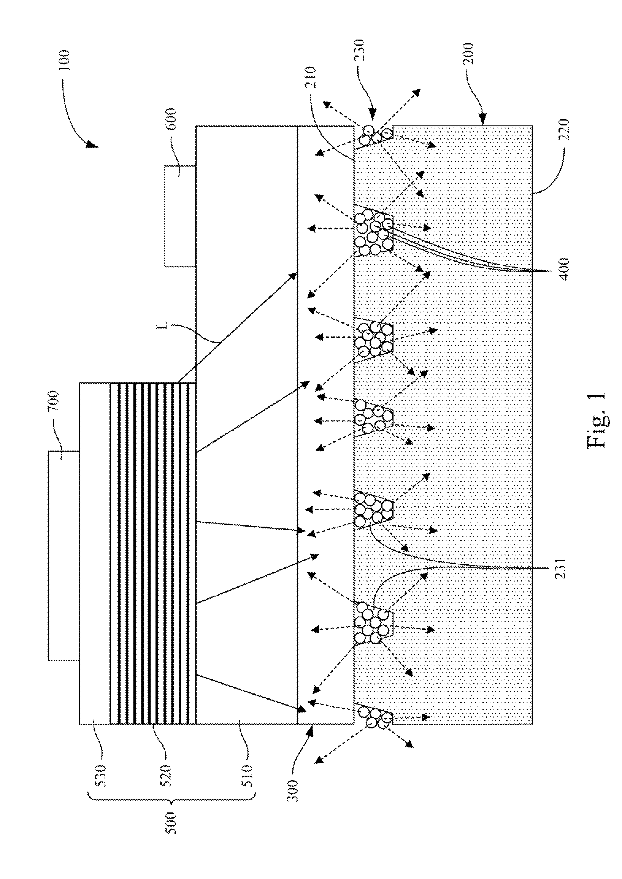
[0037]Reference is first made to FIG. 1. FIG. 1 is a side view showing the light emitting diode element 100 according to the present invention.

[0038]The present invention provides a LED element 100. The LED element 100 (or LED die) comprises a substrate 200, a buffer layer 300, a plurality of nano-spheres 400 and a light emitting structure 500. The buffer layer 300 is stacked on a surface of the substrate 200, the light emitting structure 500 is stacked on the surface of the buffer layer 300 opposite to the substrate 200, and the nano-spheres 400 are arranged in groups and at intervals on the surface of the substrate 200 which faces the buffer layer 300.

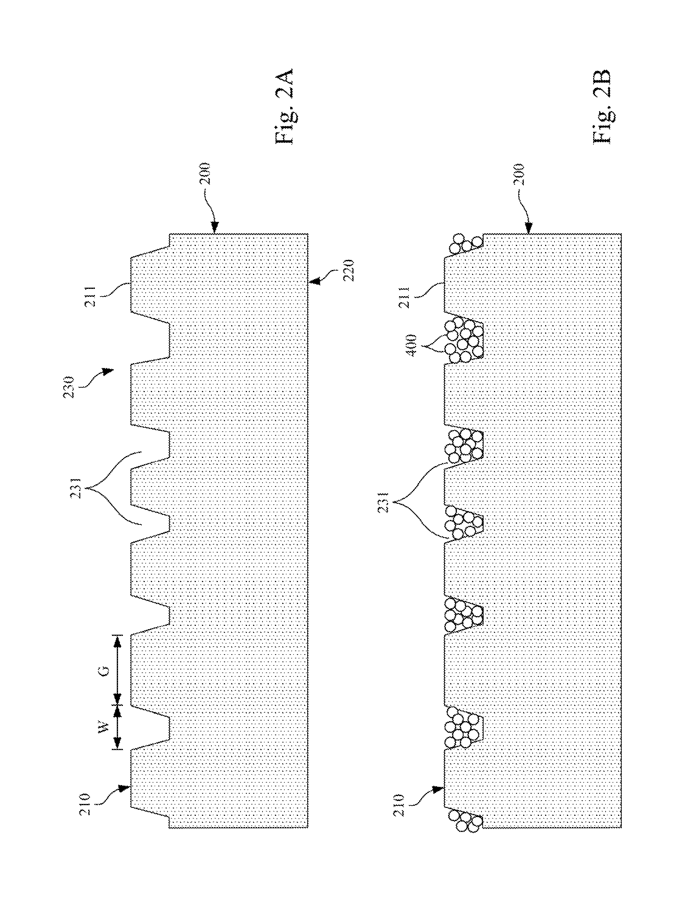
[0039]According to the first embodiment, the substrate 200 can be e.g. a sapphire substrate or a gallium nitride (GaN) substrate; however, the scope of the present invention is not limited by the mentioned substrates which only serve for illustration. The substrate 200 comprises a top surface 210 and a bottom surface 220 opposite to ...

second embodiment

[0064]FIG. 3 is a side view showing the LED element 101 according to the present invention.

[0065]The present invention provides a LED element 101. The LED element 101 (or LED die) comprises a substrate 201, a buffer layer 310, a plurality of nano-spheres 400 and a light emitting structure 500. The buffer layer 310 is disposed on the substrate 201, and a plurality of channels horizontally arranged at intervals is formed inside the buffer layer 310. The nano-spheres 400 are received in the channels 311. The light emitting structure 500 is formed on the buffer layer 310.

[0066]According to the second embodiment, the substrate 201 can be e.g. a sapphire substrate or a gallium nitride (GaN) substrate, however, the scope of the present invention is not limited by the mentioned substrates which only serve for illustration. The buffer layer 310 is e.g. a gallium nitride (GaN) layer disposed on a top surface 210 of the substrate 201 and having the same area as the top surface 210 of the subst...


PUM


Abstract

The present invention provides a light emitting diode (LED) element which comprises a substrate, a buffer layer, a plurality of nano-spheres and a light emitting structure. The substrate comprises a plurality of grooves arranged at intervals on a surface of the substrate. The buffer layer is disposed on the surface of the substrate where the grooves being formed, wherein the grooves are disposed between the substrate and the buffer layer. The nano-spheres are received in the grooves, so each groove is provided with at least a nano-sphere. The light emitting structure is disposed on the buffer layer.

Description

RELATED APPLICATIONS[0001]This application claims priority to Taiwan Application Serial Number 101116041 filed May 4, 2012, which is herein incorporated by reference.BACKGROUND[0002]1. Technical Field[0003]The present invention relates to a light emitting diode element, and more particularly to a light emitting diode element having nano-spheres.[0004]2. Description of Related Art[0005]The light emitting diode (LED) is categorized as one of the compound semiconductors, which outputs energy in a light emitting format while the electro holes of P-type and N-type semiconductor materials being combined. Moreover, in that the LED has advantages of small volume, long service life, low power consumption and fast responding, it has been widely used in like an optical display device, communication device and illumination device, and has become a must-have photoelectric element.[0006]However, confined to the structure of the conventional LED die, the light extraction efficiency of conventional...

Claims


Application Information

Patent Timeline
Patent Type & Authority Patents(United States)
IPC IPC(8): H01L33/58
CPCH01L33/22H01L2933/0091H01L33/10
Inventor CHEN, JUN-RONGYE, JHAO-CHENG
Owner LEXTAR ELECTRONICS CORP
Why Eureka
Try Eureka