Light emitting diode element
a diode element and light-emitting technology, applied in the field of light-emitting diode elements, can solve the problems of inconvenient and short-circuit dies, ineffective solution of inconvenience and shortages, and limited light extraction efficiency of conventional led dies, so as to improve the light scattering effect, improve the whole light output quality, and increase the light extraction efficiency
- Summary
- Abstract
- Description
- Claims
- Application Information
AI Technical Summary
Benefits of technology
Problems solved by technology
Method used
Image
Examples
first embodiment
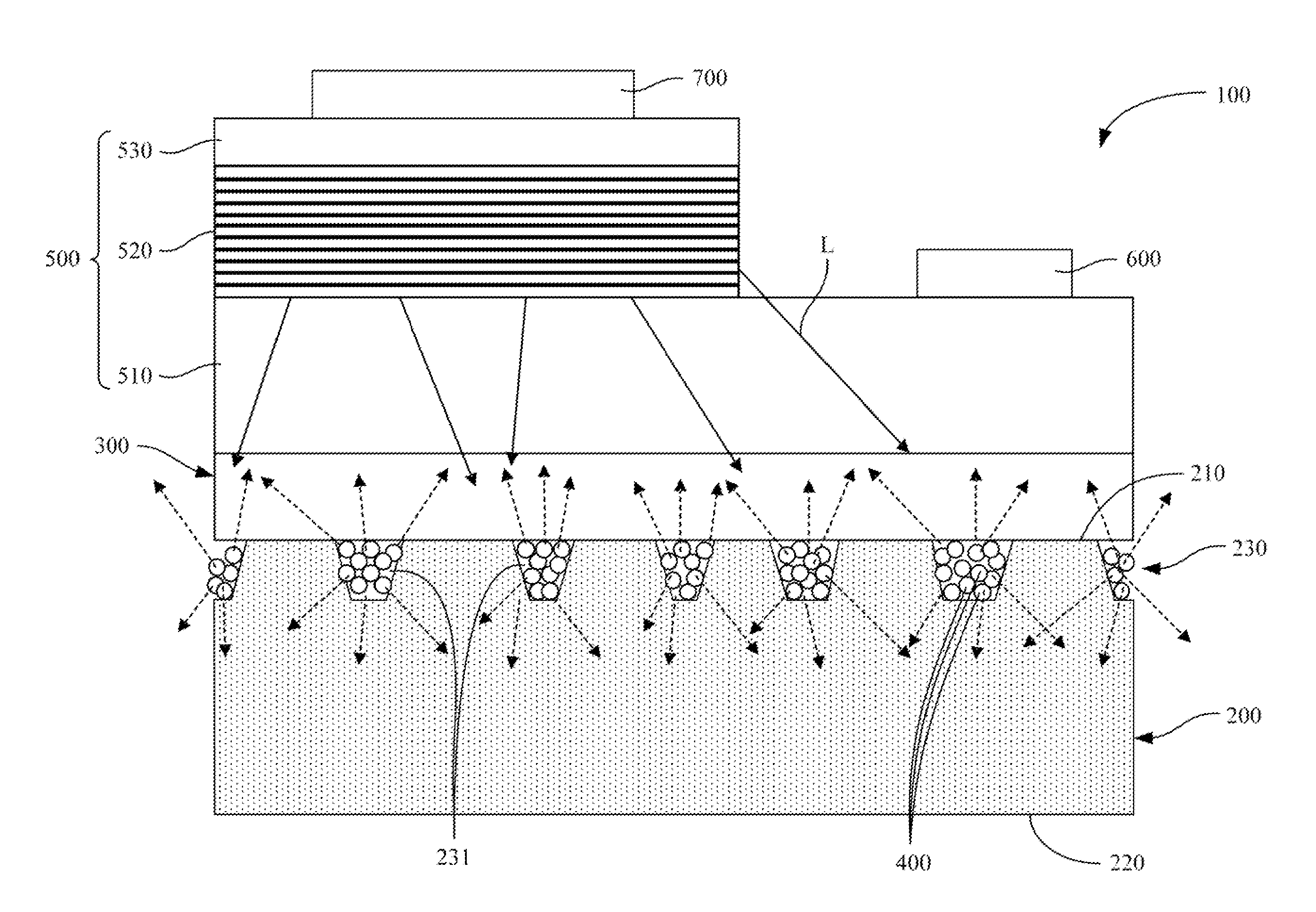
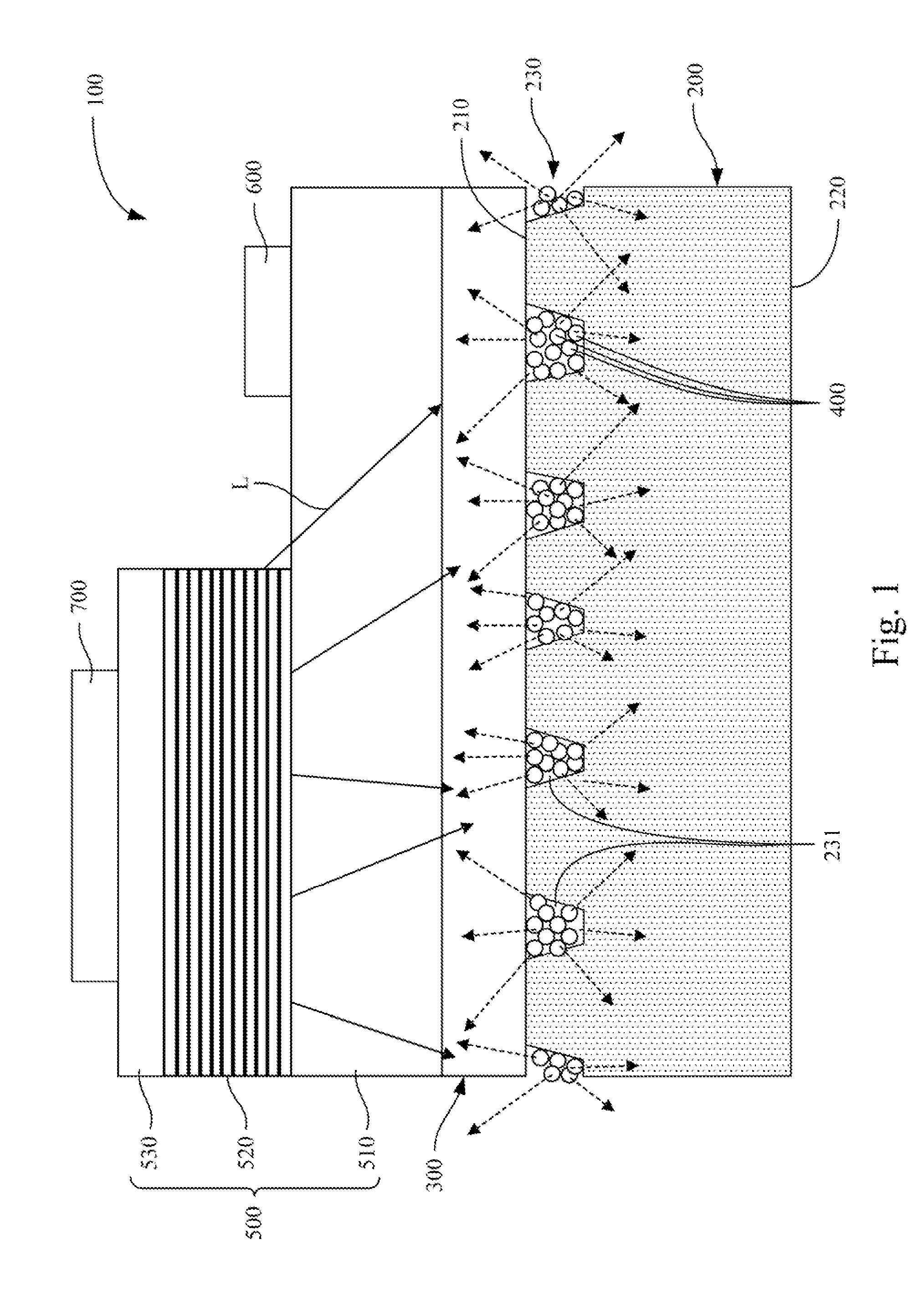
[0037]Reference is first made to FIG. 1. FIG. 1 is a side view showing the light emitting diode element 100 according to the present invention.
[0038]The present invention provides a LED element 100. The LED element 100 (or LED die) comprises a substrate 200, a buffer layer 300, a plurality of nano-spheres 400 and a light emitting structure 500. The buffer layer 300 is stacked on a surface of the substrate 200, the light emitting structure 500 is stacked on the surface of the buffer layer 300 opposite to the substrate 200, and the nano-spheres 400 are arranged in groups and at intervals on the surface of the substrate 200 which faces the buffer layer 300.
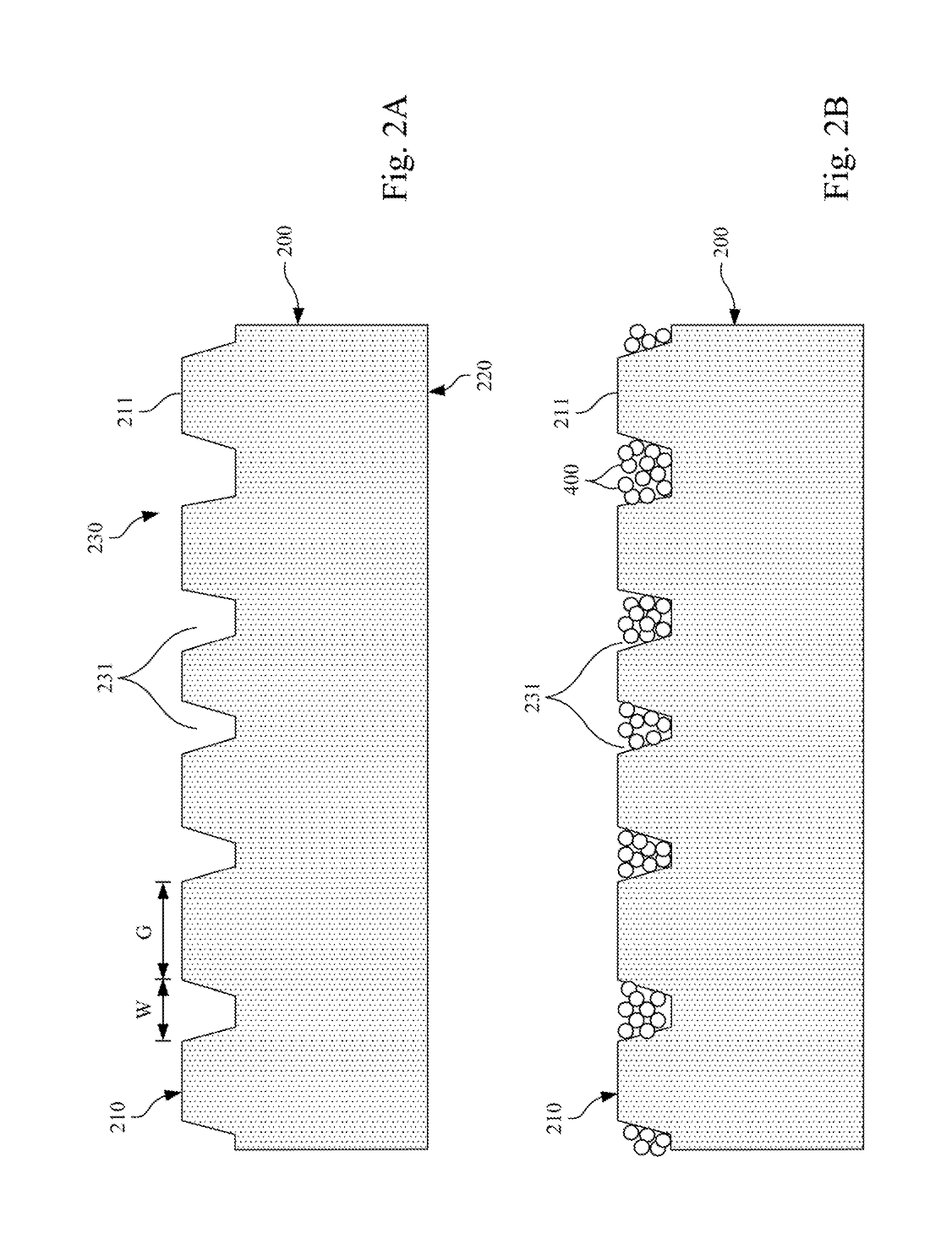
[0039]According to the first embodiment, the substrate 200 can be e.g. a sapphire substrate or a gallium nitride (GaN) substrate; however, the scope of the present invention is not limited by the mentioned substrates which only serve for illustration. The substrate 200 comprises a top surface 210 and a bottom surface 220 opposite to ...
second embodiment
[0062]FIG. 3 is a side view showing the LED element 101 according to the present invention.
[0063]The present invention provides a LED element 101. The LED element 101 (or LED die) comprises a substrate 201, a buffer layer 310, a plurality of nano-spheres 400 and a light emitting structure 500. The buffer layer 310 is disposed on the substrate 201, and a plurality of channels horizontally arranged at intervals is formed inside the buffer layer 310. The nano-spheres 400 are received in the channels 311. The light emitting structure 500 is formed on the buffer layer 310.
[0064]According to the second embodiment, the substrate 201 can be e.g. a sapphire substrate or a gallium nitride (GaN) substrate, however, the scope of the present invention is not limited by the mentioned substrates which only serve for illustration. The buffer layer 310 is e.g. a gallium nitride (GaN) layer disposed on a top surface 210 of the substrate 201 and having the same area as the top surface 210 of the subst...
PUM
 Abstract
Description
Claims
Application Information


