Semiconductor light emitting element and illuminating apparatus using the same

a technology of semiconductors and light emitting elements, applied in the direction of electrical devices, semiconductor/solid-state device manufacturing, semiconductor devices, etc., can solve the problems of difficult to obtain a reflectance higher than the natural reflectance of high reflection metals, and the method cannot be used on oxide or nitride compounds, etc., to achieve the effect of reducing power consumption, reducing energy consumption and improving brightness

Active Publication Date: 2011-01-27
PANASONIC CORP
View PDF7 Cites 47 Cited by
  • Summary
  • Abstract
  • Description
  • Claims
  • Application Information

AI Technical Summary

Benefits of technology

[0008]It is an object of the present invention to provide a semiconductor light emitting element which can improve the light extraction efficiency, and an illuminating apparatus using this element.
[0012]Therefore lights which entered the reflection film at all kinds of incident angles can be extracted efficiently, and less power consumption is needed to extract the same amount of light, and brightness can be increased with supplying the same amount of power.

Problems solved by technology

However the reflectance of a metal greatly depends on the wavelength, and this method cannot be used on oxide or nitride compound semiconductor light emitting elements which have an emission peak in the shorter wavelength side from red light.
For example, ohmic contact cannot be guaranteed between a GaN material and a high reflection metal, such as silver and aluminum.
Therefore a laminated electrode of such a metal as Ni, Pt or Rh, such a metal oxide as ITO (Indium Tin Oxide), and a high reflection metal, is used, which makes it difficult to obtain a reflectance higher than the natural reflectance of the high reflection metal.

Method used


Image

  • Semiconductor light emitting element and illuminating apparatus using the same
  • Semiconductor light emitting element and illuminating apparatus using the same
  • Semiconductor light emitting element and illuminating apparatus using the same

Examples


Embodiment Construction

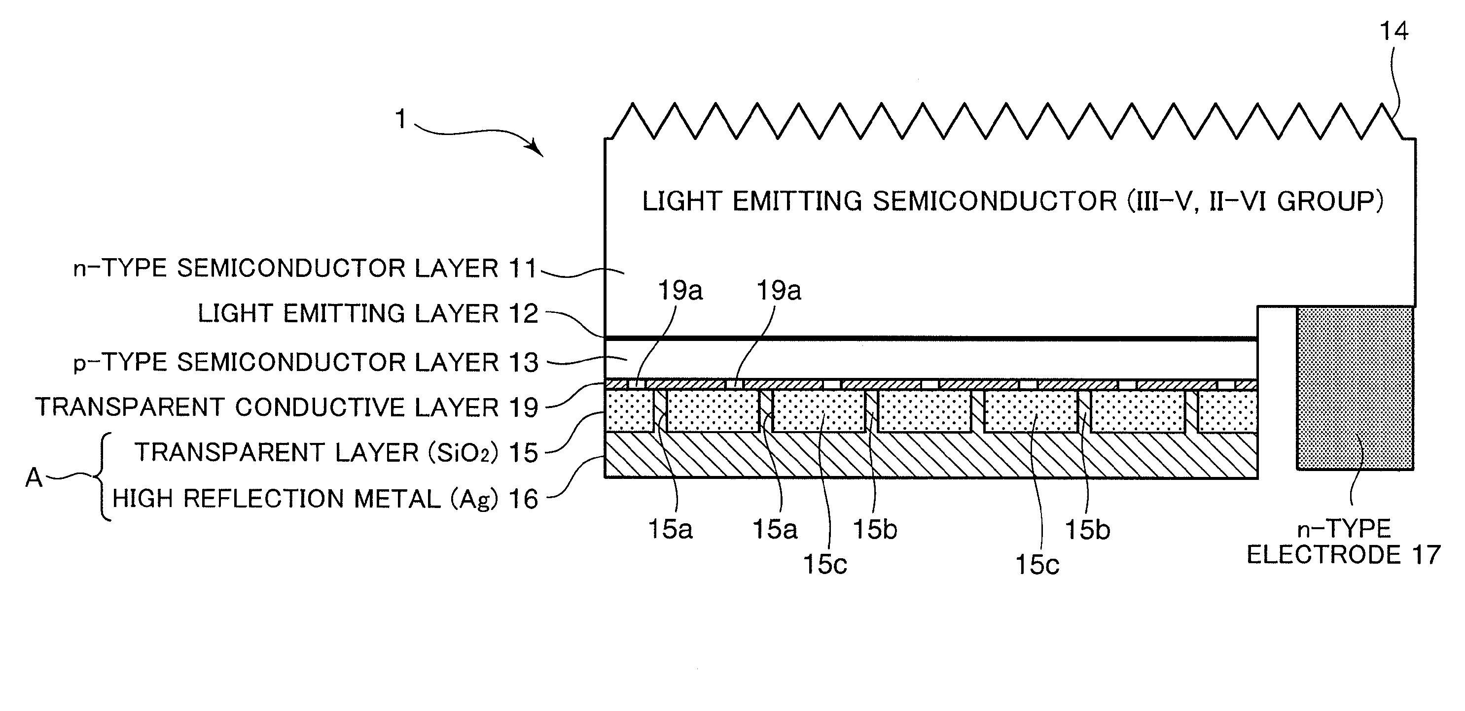
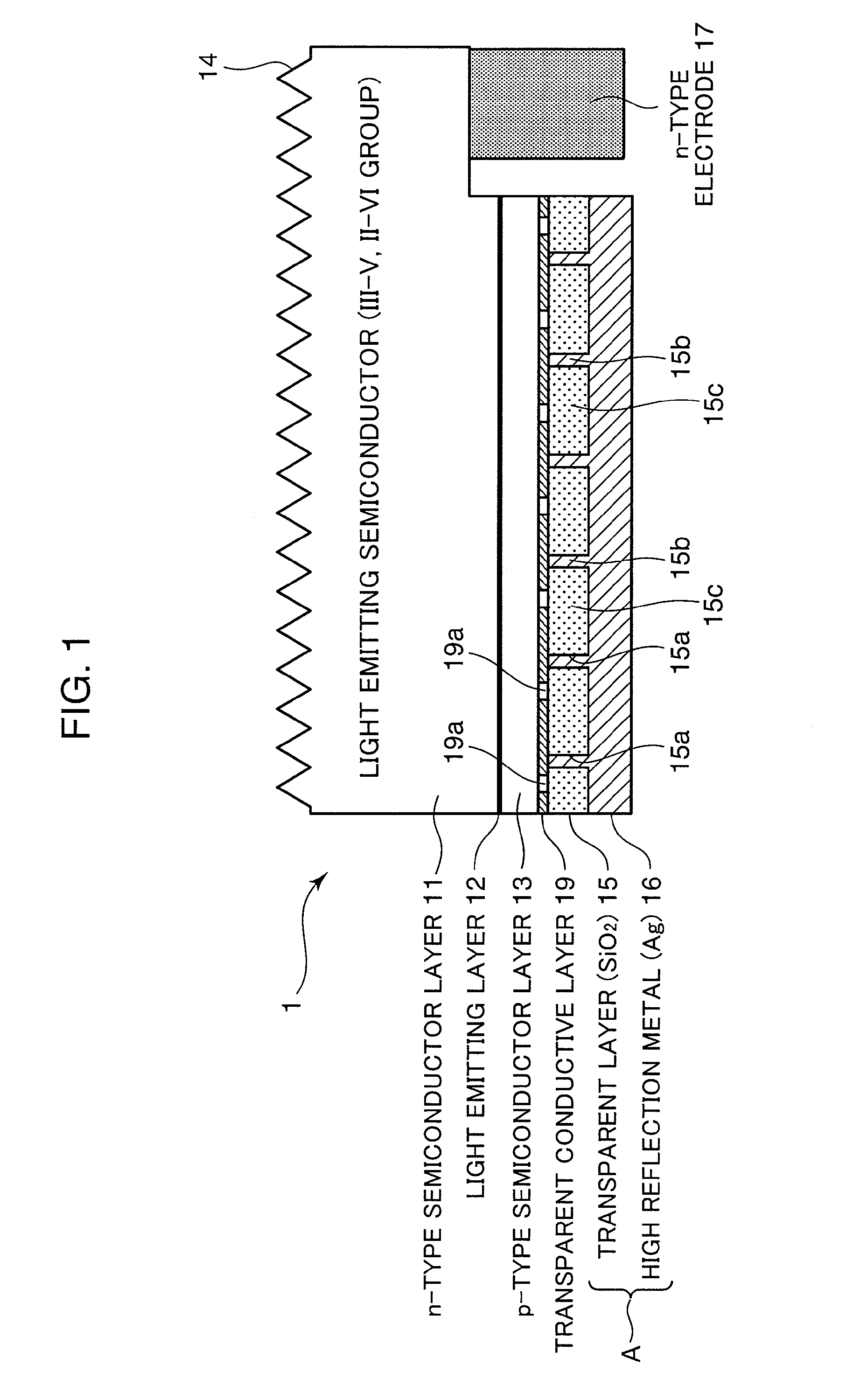
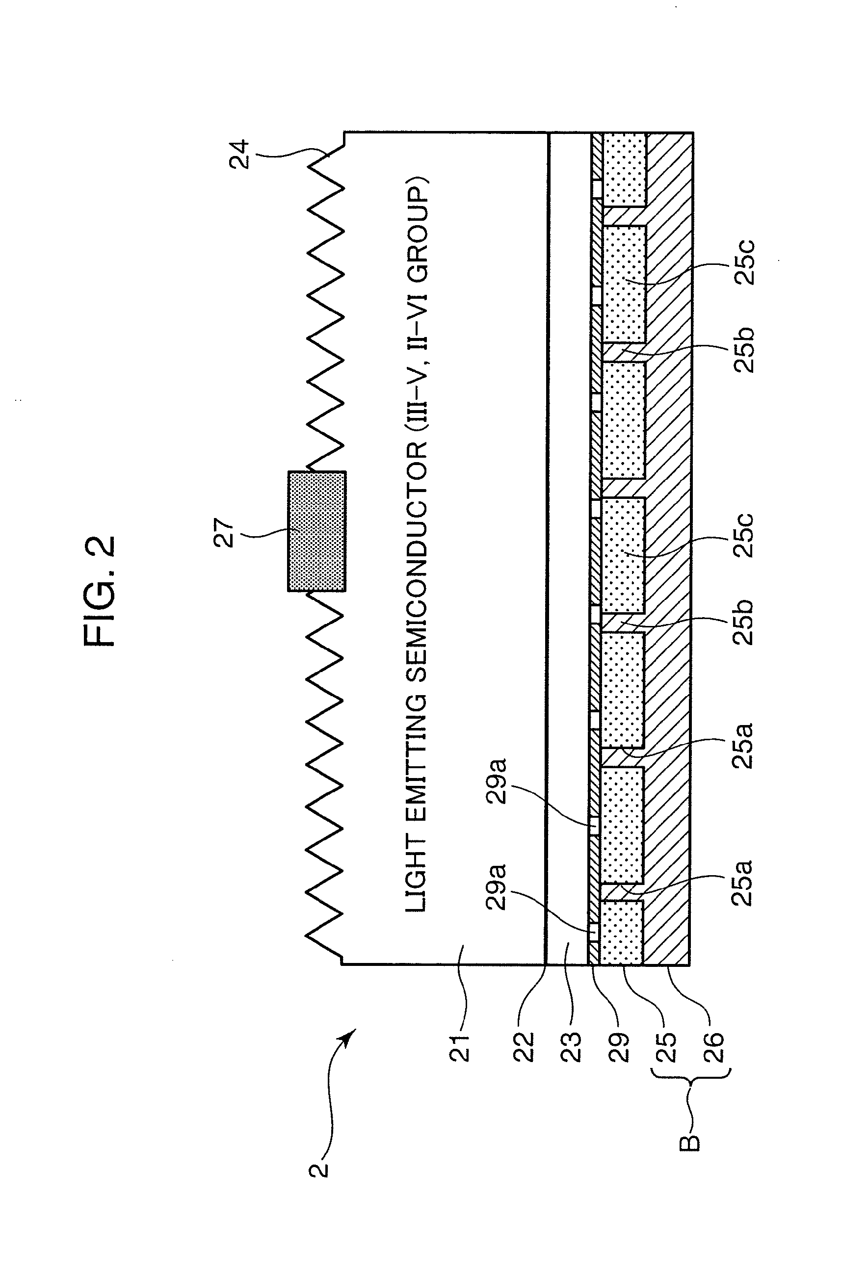
[0035]FIG. 1 to FIG. 4 are cross-sectional views depicting configurations of the light emitting diodes 1 to 4, which are semiconductor light emitting elements according to an embodiment of the present invention. The configurations in FIG. 1 to FIG. 4 are typical configuration examples of the semiconductor light emitting elements to which the present invention is applied, and the light emitting diode 1 in FIG. 1 is a flip-chip type, and the light emitting diodes 2 to 4 in FIG. 2 to FIG. 4 are wire bonding types.

[0036]The light emitting diode 1 in FIG. 1 has an n-type semiconductor layer 11, a light emitting layer 12 and a p-type semiconductor layer 13, which are laminated, and has a reflection film which is disposed on the side opposite to a surface 14 from which light emitted from the light emitting layer 12 is extracted. Noteworthy here is that the p-type electrode is the reflection film A according to the present invention. The reflection film A has: a transparent layer 15 which h...


PUM


Abstract

A semiconductor light emitting element, including: an n-type semiconductor layer having optical transparency with an emission wavelength of a light emitting layer, the light emitting layer and a p-type semiconductor layer, which are laminated; and a reflection film which is disposed on a side opposite to a surface from which light emitted from the light emitting layer is extracted, wherein the reflection film comprises: a transparent layer having optical transparency with the emission wavelength of the light emitting layer, and a metal layer, which is laminated on the transparent layer on a side opposite to the light emitting layer and is constituted by a metal material having a high reflectance, the transparent layer has a refractive index lower than a refractive index of a layer disposed on a side of the light emitting layer when viewed from the transparent layer, with the emission wavelength, and a thickness of the transparent layer is equal to or more than a value obtained by dividing a value of ¾ of the emission wavelength by the refractive index of the transparent layer.

Description

TECHNICAL FIELD [0001]The present invention relates to a semiconductor light emitting element which emits light by combining an electron and hole(s) combining in a semiconductor, and an illuminating apparatus using the semiconductor light emitting element, and more particularly to a method for improving light extraction efficiency of a semiconductor light emitting element which has an emission peak in the shorter wavelength side from red light.BACKGROUND ART[0002]In a semiconductor light emitting element in which an n-type semiconductor layer, a light emitting layer and a p-type semiconductor layer are laminated on a growth substrate having optical transparency with the emission wavelength of the light emitting layer, a method for forming a reflection film having high reflectance on the side opposite to the surface, from which the light emitted from the light emitting layer is extracted, has been used as a means of improving light extraction efficiency (or external quantum efficienc...

Claims


Application Information

Patent Timeline
Patent Type & Authority Applications(United States)
IPC IPC(8): H01L33/60H01L33/00H01L33/10H01L33/28H01L33/32H01L33/38H01L33/42H01L33/46
CPCH01L33/22H01L33/387H01L33/46H01L33/42H01L33/405
Inventor FUKSHIMA, HIROSHIYAMAE, KAZUYUKIYASUDA, MASAHARUIWAHASHI, TOMOYAMURAI, AKIHIKO
Owner PANASONIC CORP
Why Eureka
Try Eureka