Light emitting device and manufacture method thereof

a technology of light-emitting devices and manufacturing methods, which is applied in the direction of semiconductor devices, basic electric elements, electrical appliances, etc., can solve the problems of loss of market competitiveness, heat generated by leds, and inconvenient illumination of conventional leds, so as to improve light extraction efficiency, and improve light extraction efficiency

Inactive Publication Date: 2007-06-07
EPISTAR CORP
View PDF8 Cites 52 Cited by
  • Summary
  • Abstract
  • Description
  • Claims
  • Application Information

AI Technical Summary

Benefits of technology

[0010] A further another aspect of the present invention is to provide a LED with a rough surface to improve the light extraction efficiency.
[0011] A still further aspect of the present invention is to provide a LED array and a method for manufacturing the same. The LED array includes a plurality of LEDs on a substrate, and the electrodes of each LED connect directly to the circuits of the circuit board. After the plurality of LEDs are disposed on the circuit board, the substrate is removed and the surface of each LED can be further processed so as to improve the light extraction efficiency.
[0012] In one embodiment, the present invention provides a method of forming a light emitting device (LED). The method includes: (a) forming a light emitting structure, the light emitting structure including a substrate, a first conductive layer on the substrate, an active layer on the first conductive layer, and a second conductive layer on the active layer, the active layer being a light emitting layer; (b) forming a first dielectric layer on the light emitting structure; (c) forming a second dielectric layer on the first dielectric layer; (d) forming a first metal layer, the first metal layer being disposed on the light emitting structure and electrically-connected to the first conductive layer, a portion of the first metal layer being disposed on the first dielectric layer; (e) forming a second metal layer, the second metal layer being disposed on the light emitting structure and electrically-connected to the second conductive layer, a portion of the second metal layer being disposed on the first dielectric layer; (f) removing the substrate to expose a surface of the first conductive layer; and (g) roughening the surface of the first conductive layer to improve a light extraction efficiency. The first dielectric layer and the second dielectric layer electrically-isolate the first metal layer from the second metal layer. A portion of the first dielectric layer is a transparent layer, and a surface of the first dielectric layer contacting the first metal layer and / or the second metal layer is provided for reflecting the light emitted from the light emitting structure.
[0013] In another embodiment, the present invention provides a light emitting device. The LED includes a light emitting structure, a first dielectric layer, a first metal layer, a second metal layer, and a second dielectric layer. The light emitting structure includes a first conductive layer, an active layer, and a second conductive layer. The active layer is disposed on the first conductive layer and is a light emitting layer. The second conductive layer is disposed on the active layer. The first dielectric layer is disposed on the light emitting structure. The first metal layer is disposed on the light emitting structure and is electrically-connected to the first conductive layer. A portion of the first metal layer is disposed on the first dielectric layer. The second metal layer is disposed on the light emitting structure and is electrically-connected to the second conductive layer. A portion of the second metal layer is disposed on the first dielectric layer. The second dielectric layer is disposed on the first dielectric layer. The first dielectric layer and the second dielectric layer electrically-isolate the first metal layer from the second metal layer. A portion of the first dielectric layer is a transparent layer, and a surface of the first dielectric layer contacting the first metal layer and / or the second metal layer is provided for reflecting the light emitted from the light emitting structure. The first conductive layer includes a rough surface so as to improve a light extraction efficiency.

Problems solved by technology

However, conventional flip-chip LEDs still require “Dicing” and “Die Bonding” for connecting and mounting the circuit board.
Therefore, the brightness of a conventional LED is not suitable for illumination purpose.
When lots of LEDs are assembled into a LED lamp to improve the brightness, the volume of the LED lamp increases accordingly, which results in the loss of its market competitiveness.
As a result, the heat generated by the LED becomes an important issue.
“Heat” seriously affects the performance of LEDs; for example, the thermal effect influences the wavelength of lights emitted from the LED, reduces the brightness of lights generated from the semiconductor device, and damages the LED device.
Therefore, how to dissipate heat generated by the high power LED become the important issue of the LEDs.
However in US Applications Nos. 2004 / 0188696 and 2004 / 0203189, it requires drilled via array with filled metal within the sub-mount wafer and thus increases the manufacturing cost.
Furthermore, it becomes complicated to flip-chip bond each chip onto the sub-mount wafer using bonding bump.

Method used


Image

  • Light emitting device and manufacture method thereof
  • Light emitting device and manufacture method thereof
  • Light emitting device and manufacture method thereof

Examples


Embodiment Construction

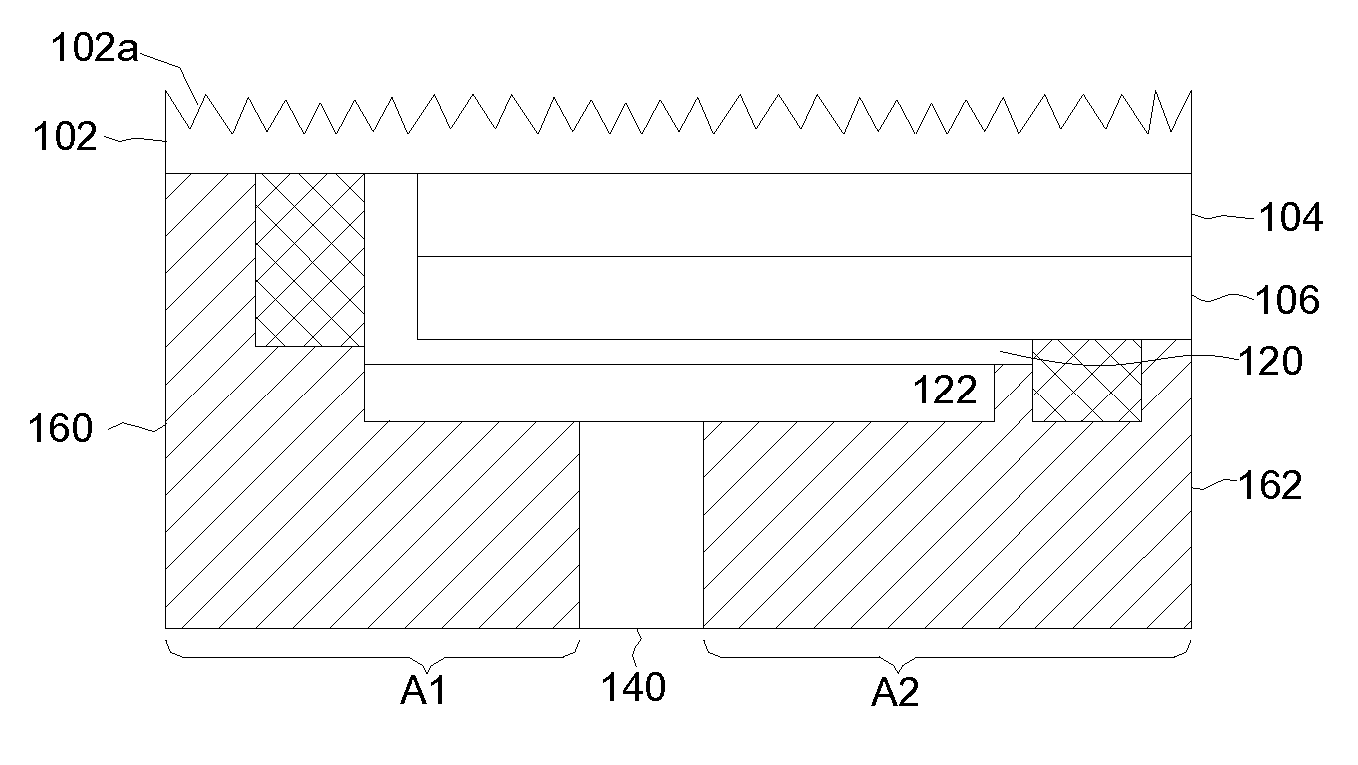
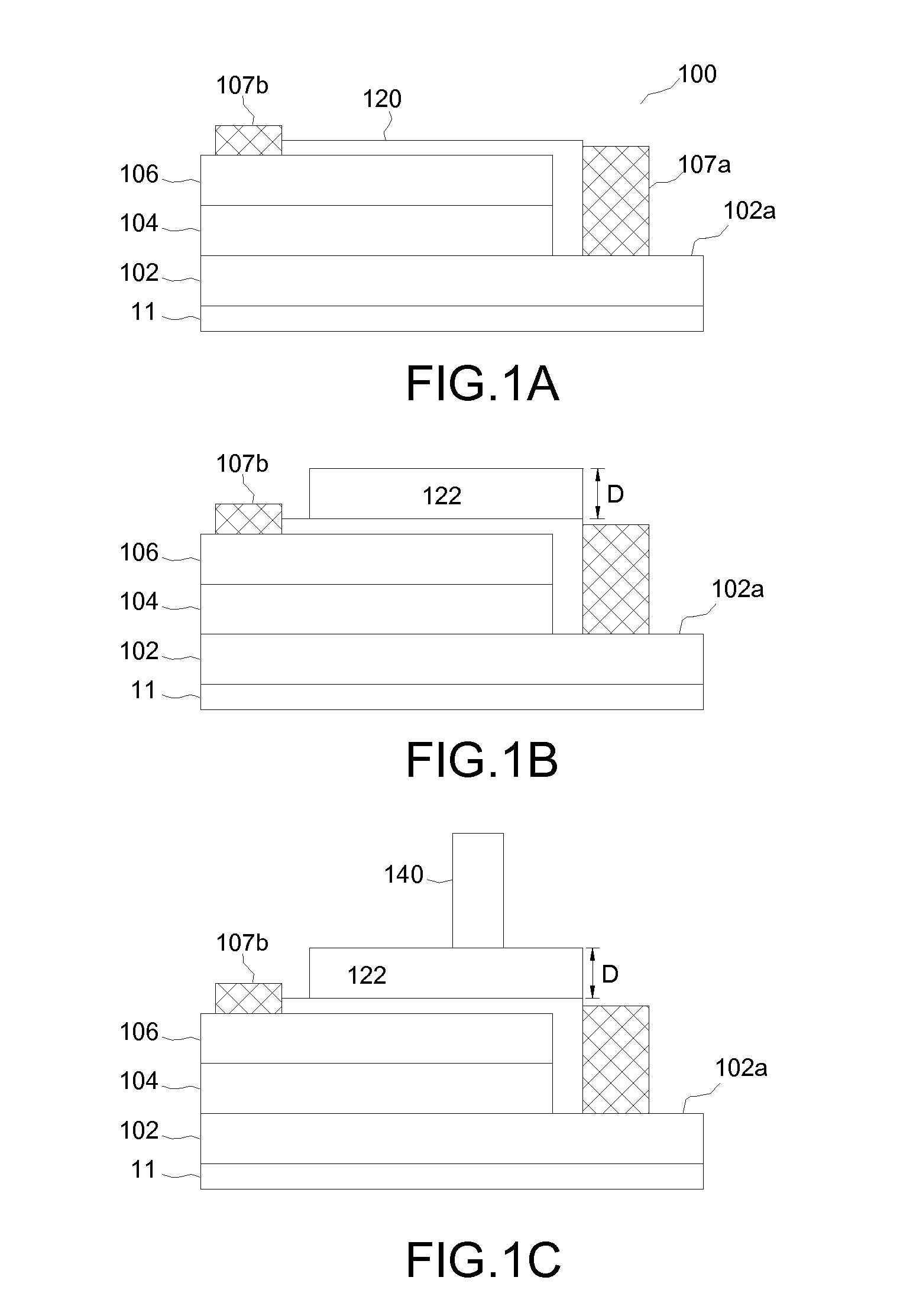
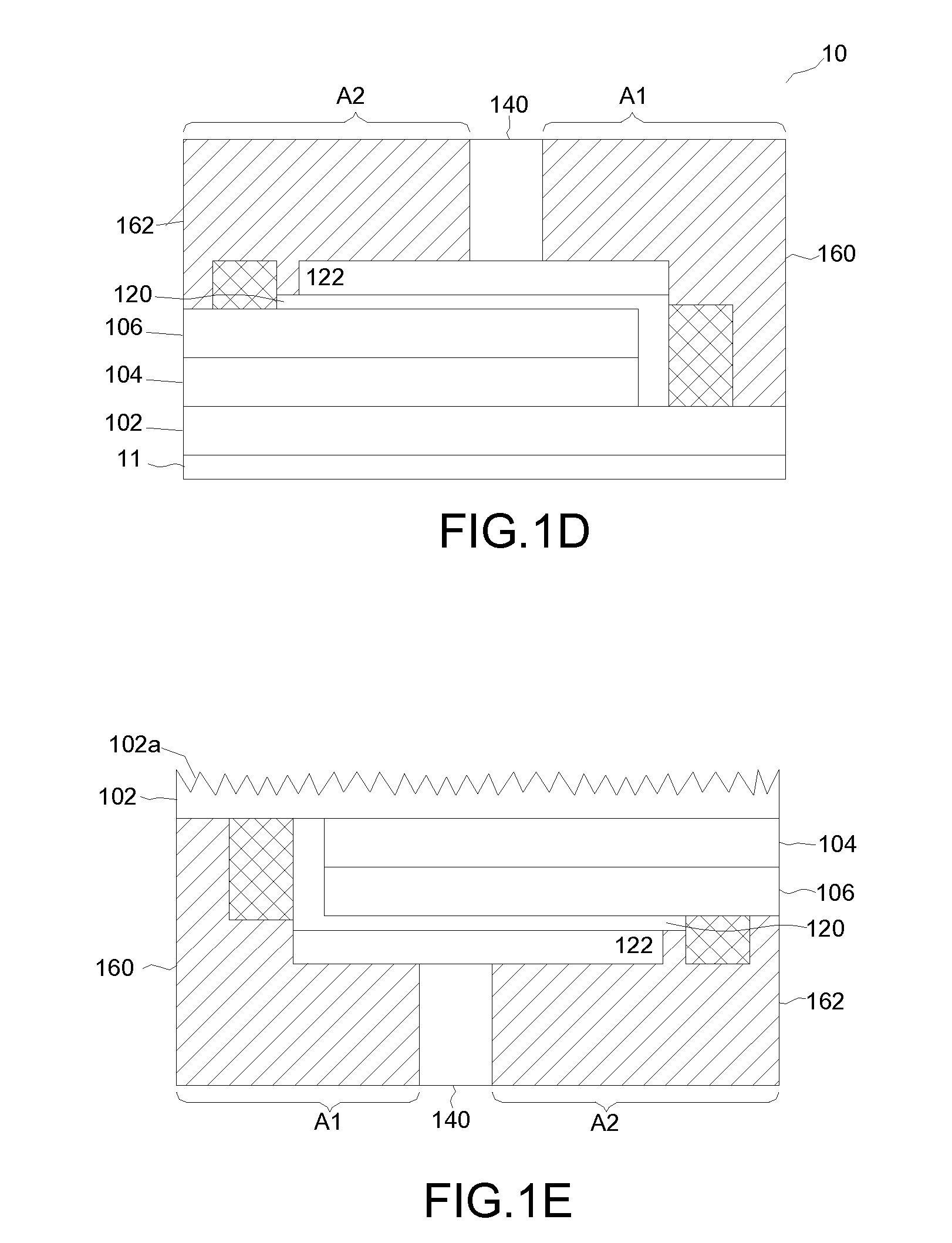
[0021]FIGS. 1A-1E illustrate the method for forming a light emitting device (LED) according to one embodiment of the present invention. Referring to FIG. 1A, at first, a light emitting structure 100 is formed. The light emitting structure 100 includes a substrate 11, a first conductive layer 102 as a cladding layer, an active layer 104 disposed on the layer 102 as a light emitting layer, and a second conductive layer 106 disposed on the layer 104 as another cladding layer. Preferably, as shown in FIG. 1A, a bonding pad 107a is disposed on an exposed portion of the layer 102, and another bonding pad 107b is disposed on the layer 106. The manufacture method and the material (e.g., Aluminum) of bonding pads 107a and 107b are well known to those skilled in the art and thus are omitted hereinafter. Furthermore, in one embodiment, the light emitting structure 100 includes a passivation layer 120 to protect the light emitting structure 100. Also, the manufacture method and the material (e....


PUM


Abstract

A flip-chip LED including a light emitting structure, a first dielectric layer, a first metal layer, a second metal layer, and a second dielectric layer is provided. The light emitting structure includes a first conductive layer, an active layer, and a second conductive layer. The active layer is disposed on the first conductive layer, and the second conductive layer is disposed on the active layer. The first metal layer is disposed on the light emitting structure and is contact with the first conductive layer, and part of the first metal layer is disposed on the first dielectric layer. The second metal layer is disposed on the light emitting structure and is in contact with the second conductive layer, and part of the second metal layer is disposed on the first dielectric layer. The second dielectric layer is disposed on the first dielectric layer. The first conductive layer includes a rough surface so as to improve a light extraction efficiency.

Description

CROSS REFERENCE TO RELATED APPLICATIONS [0001] This application claims the right of priority based on U.S. patent application Ser. No. 11 / 249,680 entitled “Light Emitting Device And Manufacture Method Thereof”, filed on Oct. 12, 2005, which claims the right of priority based on Taiwan Patent Application No. 094103370 entitled “Light Emitting Device and Manufacture Method thereof”, filed on Feb. 03, 2005, and is incorporated herein by reference and assigned to the assignee herein.FIELD OF INVENTION [0002] The present invention relates to a light emitting device and a method for manufacturing the same. In addition, the present invention relates to a light emitting device array and a method for manufacturing the same. BACKGROUND OF THE INVENTION [0003] For conventional light emitting device (LED) packages, a LED chip is mounted onto the sub-mount using the epoxy put thereon to form a LED element, and the process is called “Die Bonding”. Typically, the epoxy used in “Die Bonding” can be...

Claims


Application Information

Patent Timeline
Patent Type & Authority Applications(United States)
IPC IPC(8): H01L33/00H01L33/22
CPCH01L33/0079H01L33/22H01L33/38H01L24/13H01L24/16H01L24/81H01L25/0753H01L33/62H01L2224/131H01L2224/16227H01L2224/81005H01L2224/83104H01L33/0093H01L2924/00014H01L2924/014
Inventor CHEN, TZER-PERNGWU, JEN-CHAU
Owner EPISTAR CORP
Why Eureka
Try Eureka