Optical semiconductor device and manufacturing method thereof

a technology of optical semiconductors and manufacturing methods, applied in the direction of thermoelectric devices, electroluminescent light sources, electric lighting sources, etc., can solve the problems of large visible light reflection at the interface between these films constituting the laminated film, small brightness of the display, and large light reflection at the interface between these films. achieve the effect of suppressing the optical damage of organic el, reducing the reflectance of the encapsulating film, and improving light extraction efficiency

Inactive Publication Date: 2012-10-04
HITACHI HIGH-TECH CORP +1
View PDF7 Cites 48 Cited by
  • Summary
  • Abstract
  • Description
  • Claims
  • Application Information

AI Technical Summary

Benefits of technology

[0020]An object of the present invention is to reduce a reflectance of the encapsulating film of the optical semiconductor device and improve light extraction efficiency.
[0021]Further, another object of the present invention is to significantly suppress the optical damage to the organic EL by the optical CVD method at the time of forming the encapsulating film of the optical semiconductor device.

Problems solved by technology

However, since the silicon oxide film and the silicon nitride film are greatly different from each other in terms of refractive index, the laminated film thereof has a problem that a reflection of visible light occurring at the interface between these films constituting the laminated film is large.
More specifically, when the encapsulating film composed of a silicon oxide film and a silicon nitride film is adopted for the top emission type organic EL display panel, since an extraction efficiency of the visible light emitted on the organic EL layer is small, there arises a problem that the brightness (light extraction efficiency) of the display is small.

Method used


Image

  • Optical semiconductor device and manufacturing method thereof
  • Optical semiconductor device and manufacturing method thereof
  • Optical semiconductor device and manufacturing method thereof

Examples


Embodiment Construction

[0044]Hereinafter, embodiments of the present invention will be described in detail with reference to the accompanying drawings. Note that components having the same function are denoted by the same reference symbols throughout the drawings for describing the embodiments, and the repetitive description thereof will be omitted. In addition, the description of the same or similar portions is not repeated in principle unless particularly required in the following embodiments.

[0045]An embodiment of the present invention will be described below with reference to the drawings.

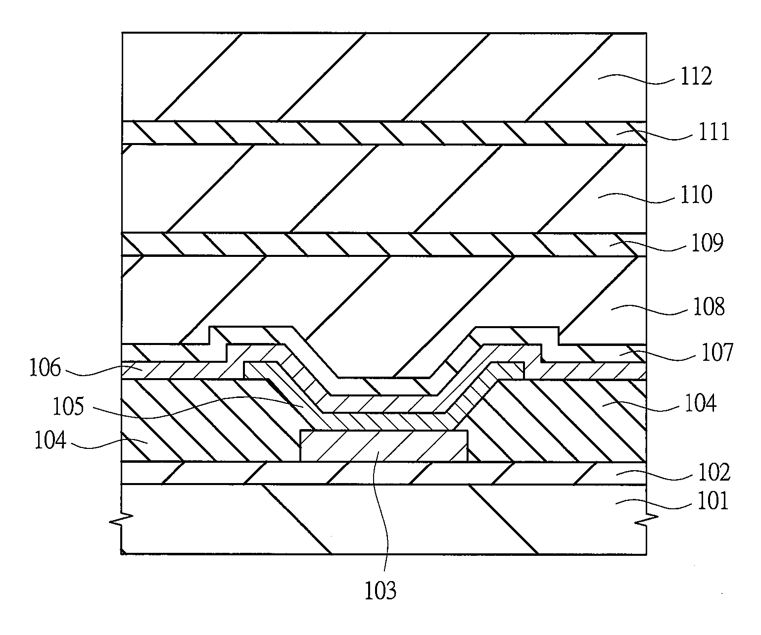
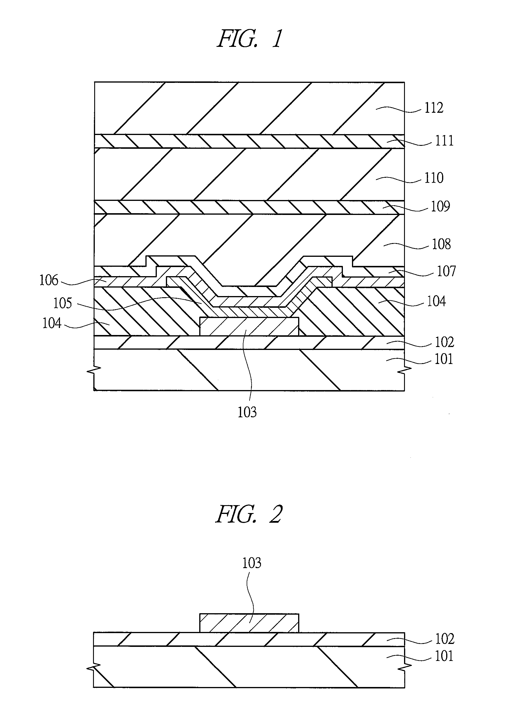
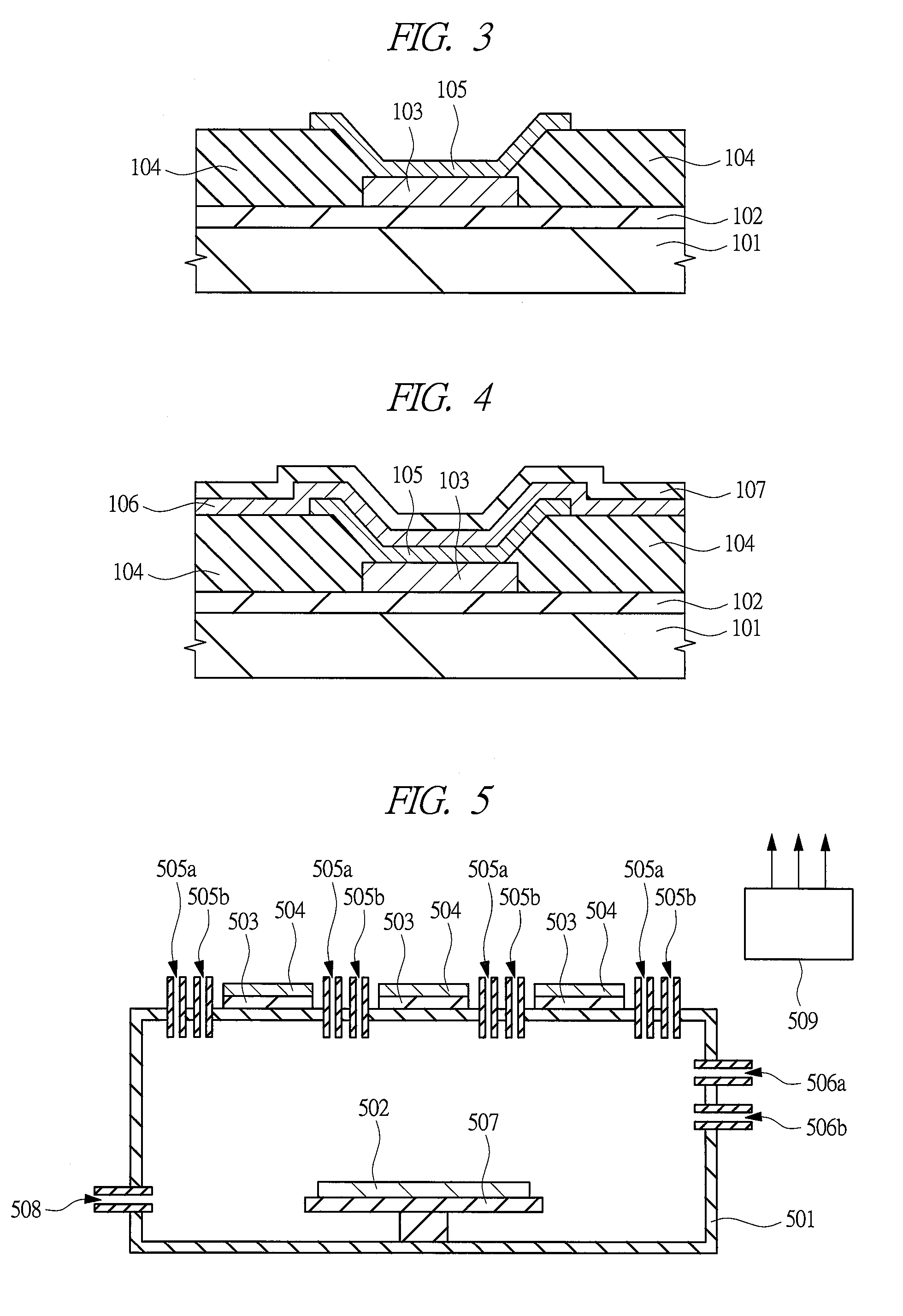
[0046]FIG. 1 shows a cross-sectional view of an optical semiconductor device including an organic EL element of the present embodiment. The organic EL element of the present embodiment has a glass substrate 101 as shown in FIG. 1, and an anode electrode 103 and a bank part 104 are formed on the glass substrate 101 via an insulating film 102. The glass substrate 101 contains, for example, quartz, and the insulating fi...


PUM

PropertyMeasurementUnit
refractive indexaaaaaaaaaa
thicknessesaaaaaaaaaa

Abstract

In a device having an anode electrode, an organic EL layer, and a cathode electrode formed on a substrate in this order from a main surface side of the substrate, and an encapsulating film provided on the substrate so as to cover the emission layer, the encapsulating film includes a laminated film obtained by alternately laminating buffer films serving as flattening films and barrier films having high moisture barrier property, and the flattening film and the barrier film include a silicon oxynitride film. In the manufacturing process of the device, the buffer film including silicon oxynitride is formed by an optical CVD method using vacuum ultraviolet light, and in this process, radical irradiation by remote plasma is performed during the irradiation of the vacuum ultraviolet light.

Description

CROSS-REFERENCE TO RELATED APPLICATION[0001]The present application claims priority from Japanese Patent Application No. 2011-081553 filed on Apr. 1, 2011, the content of which is hereby incorporated by reference to this application.TECHNICAL FIELD OF THE INVENTION[0002]The present invention relates to an optical semiconductor device and a manufacturing method thereof, and in particular, to an encapsulating film of an overall organic EL element and a manufacturing method thereof.BACKGROUND OF THE INVENTION[0003]An organic electroluminescence (hereinafter, organic EL) element has many merits such as low power consumption, self-luminescence, and high-speed response, and the development of the organic EL has been pursued for the application to a flat panel display (FPD) or lighting equipment. Further, a bendable display device can be achieved by using a flexible substrate such as a resin substrate (including a resin film), and new added values such as lightness in weight and unbreakabi...

Claims


Application Information

Patent Timeline
Patent Type & Authority Applications(United States)
IPC IPC(8): H01L51/52H01L51/56
CPCH01L51/5256H10K50/8445H05B33/04H10K50/85H10K50/844H10K71/00
Inventor MINE, TOSHIYUKIFUJIMORI, MASAAKIOHASHI, NAOFUMI
Owner HITACHI HIGH-TECH CORP
Why Eureka
Try Eureka