Phosphor single crystal substrate and method for preparing the same, and nitride semiconductor component using the same

a single crystal substrate and phosphor technology, applied in the direction of crystal growth process, polycrystalline material growth, chemically reactive gases, etc., can solve the problems of low spectral reflectance, low crystalline quality of phosphor produced, unsatisfactory light emission of phosphor, etc., to improve the growth rate of seeds, improve the effect of cooling function and easy production

Inactive Publication Date: 2006-03-16
AMMONO SP Z O O (PL) +1
View PDF97 Cites 69 Cited by
  • Summary
  • Abstract
  • Description
  • Claims
  • Application Information

AI Technical Summary

Benefits of technology

[0022] In the area of the convection control means 2, it is preferable that the cooling device 6 is arranged for cooling so that it is easier to make a predetermined temperature difference between the dissolution zone 13 and the crystallization 14. It is also preferable that the cooling device 18, which can cool the bottom of the flowing area of the crystallization zone, is placed in the autoclave and thereby rapid c

Problems solved by technology

In this procedure the nitride reaction of gallium oxide occurred indeed on a surface of grains, however there are a lot of problems with reaching a 100% yield.
Additionally, the phosphor produced has a low crystalline quality and a

Method used


Image

  • Phosphor single crystal substrate and method for preparing the same, and nitride semiconductor component using the same
  • Phosphor single crystal substrate and method for preparing the same, and nitride semiconductor component using the same
  • Phosphor single crystal substrate and method for preparing the same, and nitride semiconductor component using the same

Examples


example

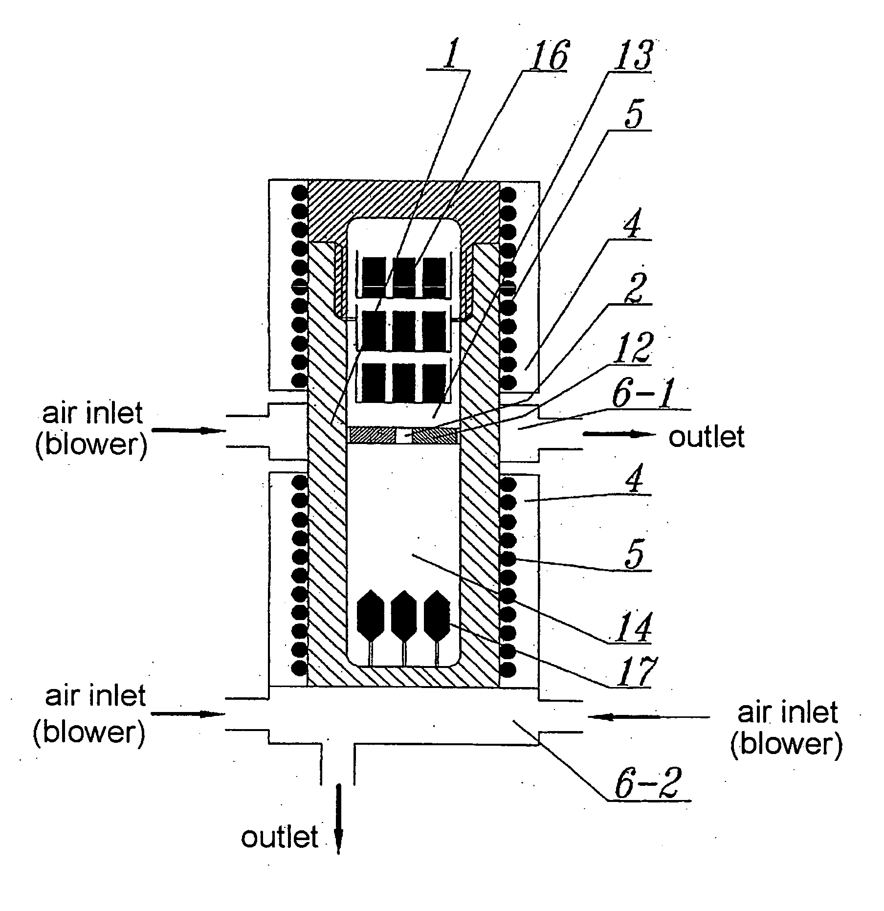
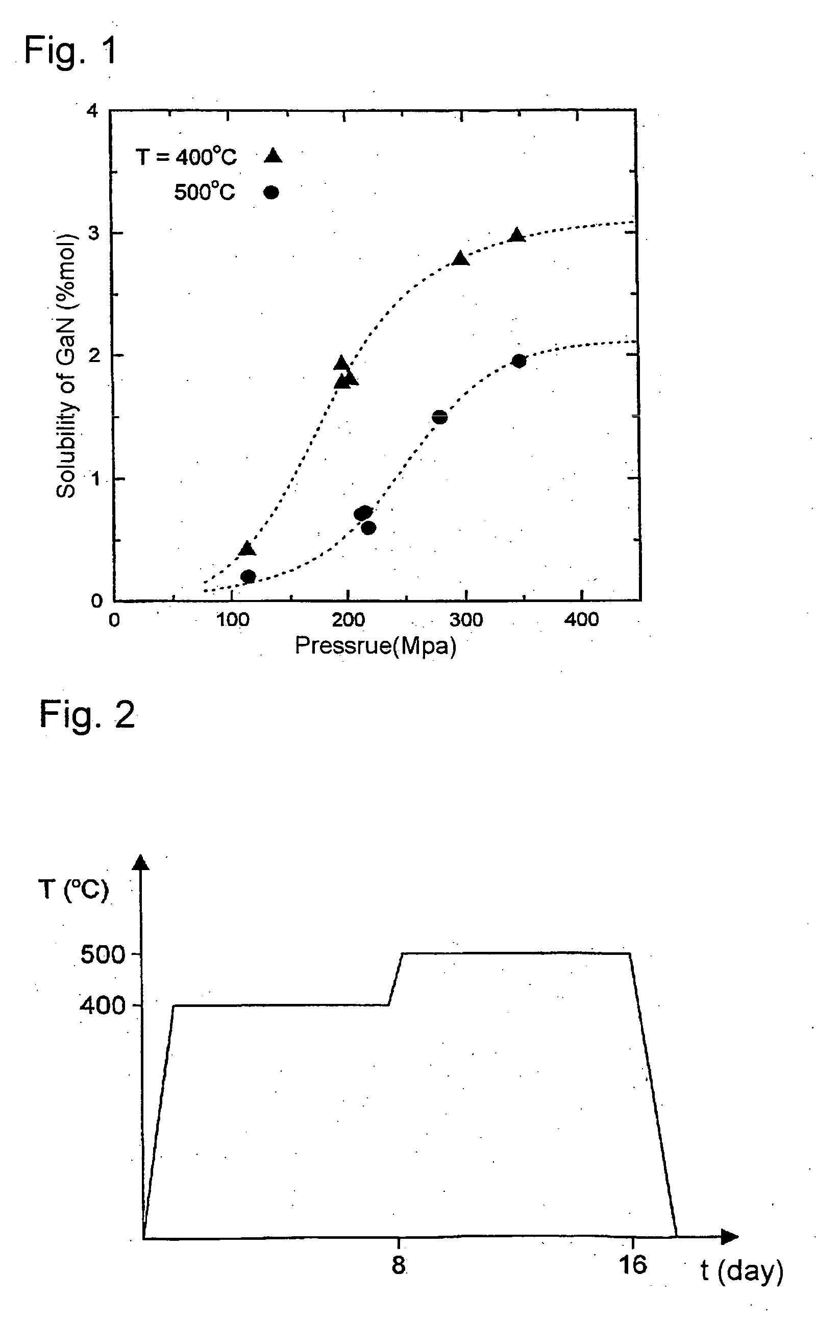
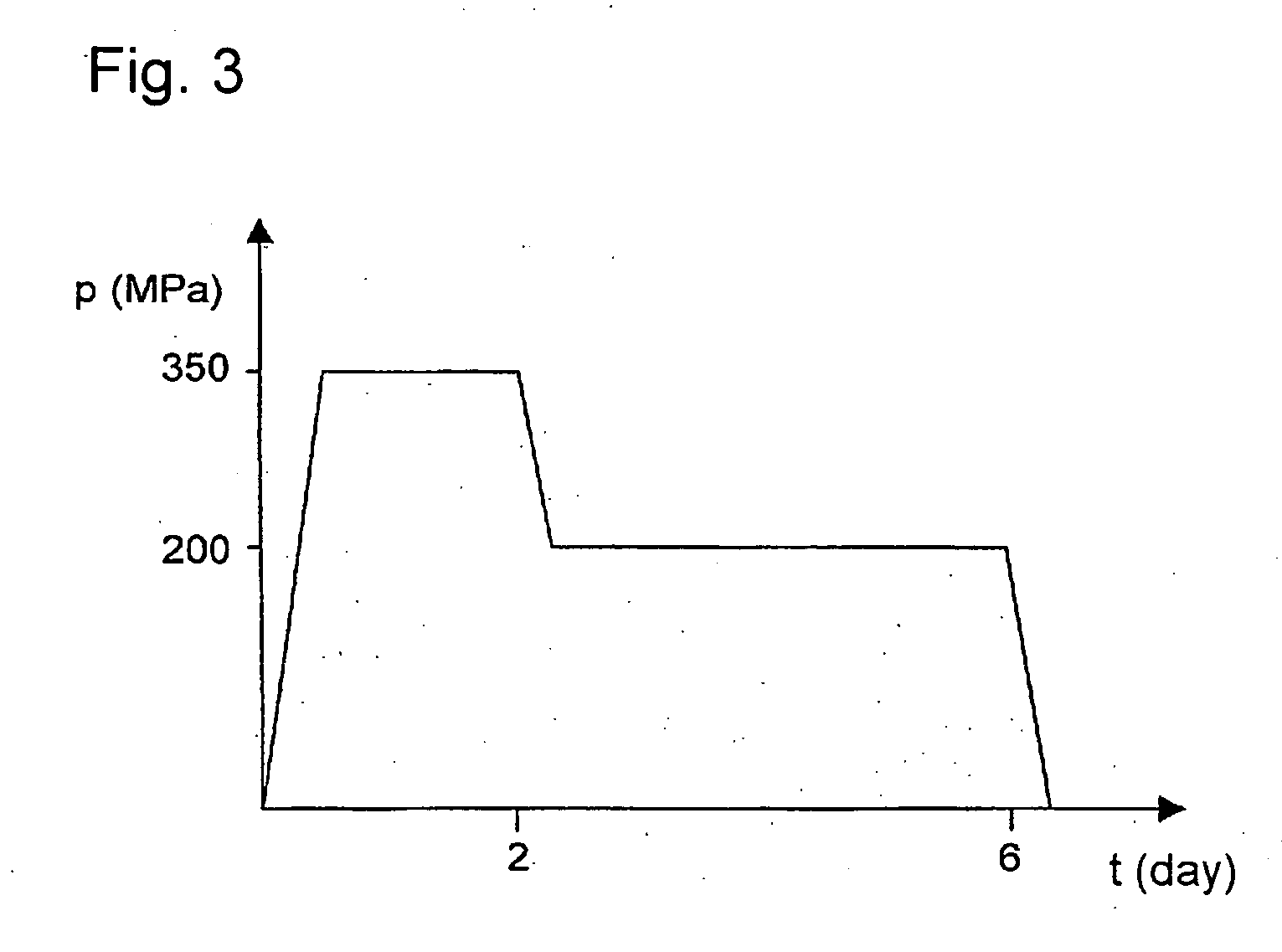
[0080] High-pressure autoclave 1 (FIG. 4 and 5), having the inner diameter of 40 mm, length equal to 480 mm (D / L= 1 / 12) and volume of 585 cm3, is charged with 30 g of feedstock in the form of GaN in the crucible in the dissolution zone 13, and GaN seed of the diameter of 1 inchφ obtained by HVPE method is placed in the crystallization zone 14 of the same autoclave. Next the autoclave 1 is filled with 1.2 g of 6N purity metallic gallium and 1.2 g of metallic Zn, and then 7 g of 3N purity metallic lithium (or 23 g of metallic sodium) as a mineralizer, and further 238 g of ammonia (SN) and finally closed. The autoclave 1 is introduced into the furnace unit 4 and heated to 200° C. for three days.

[0081] Then the temperature in the dissolution zone 13 of the autoclave is increased to 425° C., while the temperature in the crystallization zone 14 is increased to 525° C. The resultant pressure within the autoclave is 2.5 kbar. The autoclave is left under such condition for another twenty ei...

example 2

[0099] The light emitting device obtained in Example 1 is made in the form of flip chip type, then the light emitting device having the other phosphor is formed. The other phosphor can be formed by coating the surface of the light extraction plane of the phosphor substrate or by molding the resin mixed with phosphor. According to this Example, light emitting device (101, 102) is made in the form of flip chip type and nitride phosphor layer 103 of (Ca0.97Eu0.03)2Si5N8 is coated by spray coating or screen print on the surface of the light extraction plane of the phosphor substrate of the light emitting device so as to obtain a white light resource. (FIG. 12)

example 3

[0100] The light emitting device obtained in Example 1 is made in the form of flip chip type using the yttrium-gadolinium-aluminum oxide phosphor activated by Cerium (Y—Gd—Al—O:Ce) as a phosphor coating the surface of the substrate of the light emitting device by spray coaring or screen print so as to obtain a white light resource.


PUM


Abstract

A light emitting device having a phosphor substrate, which comprises nitride containing at least one element selected from Group XIII (IUPAC 1989) having a general formula XN, wherein X is at least one element selected from B, Al, Ga and In, a general formula XN:Y, wherein X is at least one element selected from B, Al, Ga and In, and Y is at least one element selected from Be, Mg, Ca, Sr, Ba, Zn, Cd and Hg, or a general formula XN:Y,Z, wherein X is at least one element selected from B, Al, Ga and In, Y is at least one element selected from Be, Mg, Ca, Sr, Ba, Zn, Cd and Hg, and Z is at least one element selected from C, Si, Ge, Sn, Pb, O and S. The phosphor substrate is prepared by crystallization from supercritical ammonia-containing solution and the light emitting device is formed by a vapor phase growth on the phosphor substrate so as to obtain a light emitting device which has a wavelength distribution emitting a white light etc. and a good yield.

Description

TECHNICAL FIELD [0001] The present invention relates to a phosphor bulk single crystal substrate formed by crystallization from supercritical solution and a method for preparing the same, and a light emitting device using the substrate. BACKGROUND ART [0002] To realize the white light emitting from blue light emitting by converting a wavelength from a nitride semiconductor light emitting device, a device of combination with a gallium nitride light emitting device and YAG:Ce phosphor is proposed. The mechanism for obtaining the white light from emitting device of converting a wavelength generally comprises steps of mixing phosphor powder into coating of LED chip or mold resin, absorbing a part of the emitted light from the chip into the phosphor, exciting a phosphor, mixing the excited light from the phosphor with the emitted light from the chip which is not absorbed, and forming a mixed colored light. [0003] However, the method for manufacturing the phosphor layer using the phosphor...

Claims


Application Information

Patent Timeline
IPC IPC(8): C30B15/14C30B7/00C30B7/10C30B9/00C30B25/18C30B29/02C30B29/40H01L33/32H01L33/50
CPCC30B7/00C30B7/10C30B25/18H01L33/32C30B29/403C30B29/406H01L33/08C30B29/02
Inventor DWILINSKI, ROBERTDORADZINSKI, ROMANGARCZYNSKI, JERZYSIERZPUTOWSKI, LESZEKKANBARA, YASUO
Owner AMMONO SP Z O O (PL)
Why Eureka
Try Eureka