Light-emitting devices with high extraction efficiency

a light-emitting device and high-efficiency technology, applied in the direction of semiconductor devices, basic electric elements, electrical appliances, etc., can solve the problems of increased total internal reflection (“tir”), serious deterioration of total luminescent efficiency, and too-large difference of refractive indices of interfaces, so as to improve the light extraction efficiency of the light-emitting device

Inactive Publication Date: 2007-02-08
SU JUNG CHIEH
View PDF7 Cites 51 Cited by
  • Summary
  • Abstract
  • Description
  • Claims
  • Application Information

AI Technical Summary

Benefits of technology

[0014] It is an object of the present invention to convert part of the light captured / trapped by the total internal reflection phenomenon into the transmitted light via the light-tunneling effect, thereby improving the light extraction efficiency of a light-emitting device. In particular, the present invention causes the light with an incident angle larger than the total reflection angle to induce light-tunneling effect by utilizing a light-tunneling layer structure to form a light control portion so as to increase the light extraction efficiency.

Problems solved by technology

Thus, losses due to the total internal reflection (“TIR”) increase rapidly with the ratio of the refractive index inside the device to that outside the device.
Specifically, for a cubic shaped device, there are six such interfaces or escape cones and the loss should be six times. Therefore, serious deterioration of the total luminescent efficiency occurs.
The too-large difference of refractive indices of the interface is the major problem encountered by EL light-emitting devices.
Both methods critically depend on the materials used and their complicated manufacturing process of optical multi-layers, and therefore their costs and optical characteristics cannot be controlled effectively in mass production.

Method used


Image

  • Light-emitting devices with high extraction efficiency
  • Light-emitting devices with high extraction efficiency
  • Light-emitting devices with high extraction efficiency

Examples


Embodiment Construction

[0035] The present invention is described in more detail by referring to the accompanying drawings. The drawings are to describe the preferred embodiments. However, the present invention is exemplified with several embodiments but is not limited by said embodiments. Said embodiments are to disclose the scope of protection of the present invention to persons of ordinary skill in the art in more detail.

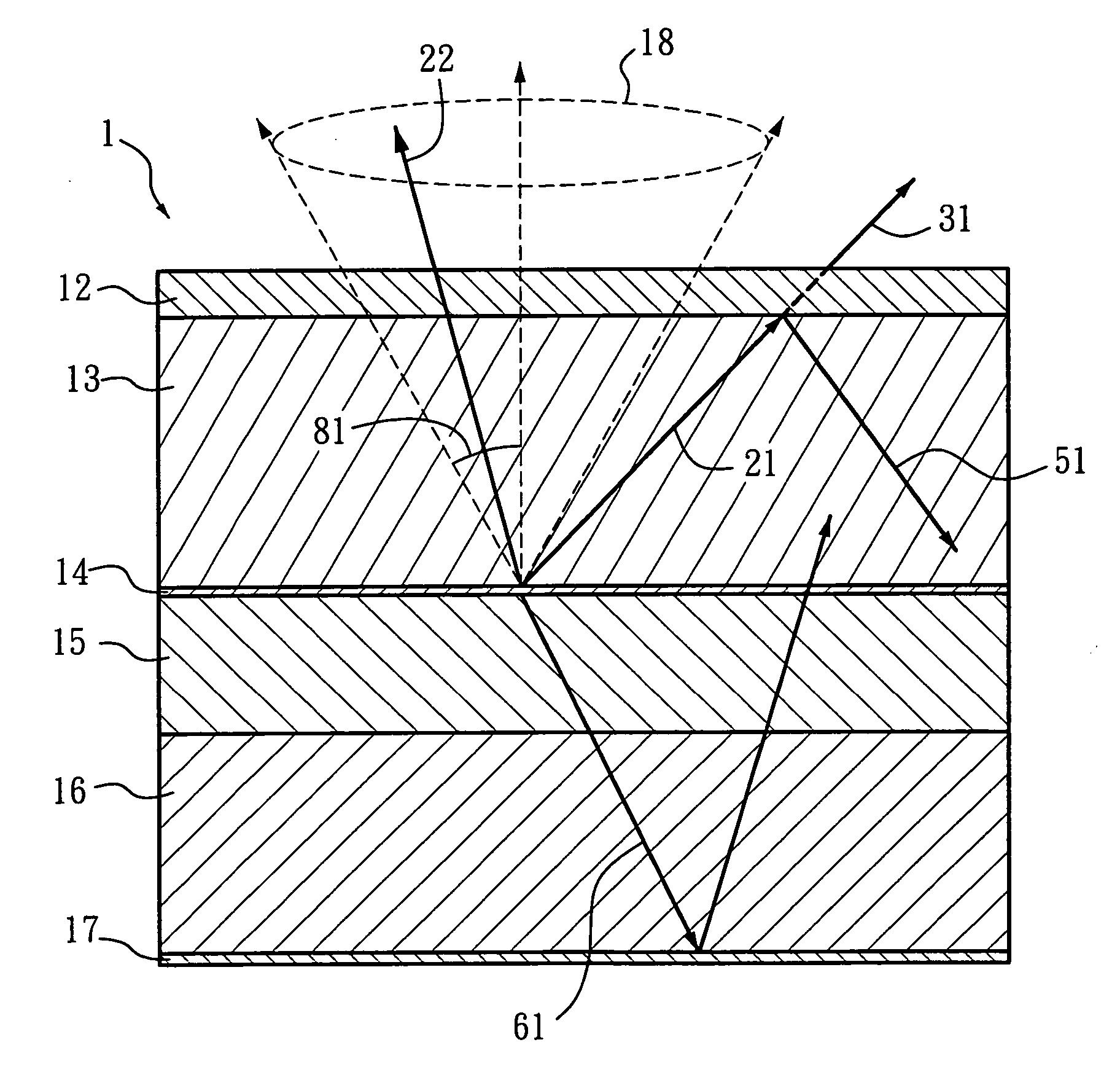
[0036] According to the present invention, a light-emitting device represents an organic / inorganic electro-luminance light-emitting device with at least one light-emitting layer that can emit light or generate light by applying external power. More specifically, the refractive index is aimed at the peak wavelength of the major emitted light generated by the light-emitting layer. The light-tunneling layer refers to a dielectric layer with a refractive index lower than that of the light-exiting surface layer of the light-emitting device. Said layer is disposed on the light-exiting surfac...


PUM


Abstract

The present invention relates to a light-emitting device having a substrate and a light-emitting layer comprising an electroluminescent material, wherein the light-emitting layer (p-n junction) is sandwiched between a p-type cladding layer with a p-electrode layer and an n-type cladding layer with an n-electrode layer. The light-emitting device is characterized in that a light control portion is deposited on a light-exiting surface of the light-emitting device. Said light control portion comprises at least one light-tunneling layer. Said light-tunneling layer has a refractive index with respect to the wavelength of the main emitting-light from the light-emitting layer lower than the refractive indices of the substrate, the cladding layers and the electrode layers. The light extraction efficiency is increased by the light tunneling effect when the emitting-light emitted by the light-emitting layer enters the interface between the epitaxial layer and the surrounding material with an incident angle larger than the critical angle. The tunneling light from the light control portion can be polarized, such that a polarized light-emitting device can be realized in practice.

Description

BACKGROUND OF THE INVENTION [0001] 1. Field of the Invention [0002] The present invention relates to a light-emitting device, such as a light-emitting diode (LED), a resonant cavity LED and a flat-surface type LED (for example, an organic LED (OLED)). In particular, the present invention relates to a semiconductor light-emitting device with a light control portion at least constituted by a light-tunneling layer. [0003] 2. Related Art [0004] An electroluminescence (EL) light-emitting device basically comprises a light-emitting portion, which essentially consists of an active layer and cladding layers, with materials capable of operating from near ultraviolet (UV) spectrum to infrared (IR) spectrum. The materials include groups III-V and II-VI semiconductors, semi-conducting polymers and particular binary, ternary and quaternary alloy materials, such as III-Nitride, III-Phosphides and III-Arsenides (for example, GaN, AlGaN, AlInGaN, AlGaInP, GaAlP, GaAsP, GaAs and AlGaAs). A semicondu...

Claims


Application Information

Patent Timeline
Patent Type & Authority Applications(United States)
IPC IPC(8): H01L33/00H01L33/22H01L33/04H01L33/32H01L33/44
CPCH01L33/02H01L51/5275H01L33/44H10K50/858
Inventor SU, JUNG-CHIEH
Owner SU JUNG CHIEH
Why Eureka
Try Eureka