Semiconductor light-emitting device and method for manufacturing semiconductor light-emitting device

a technology of semiconductor light-emitting device and semiconductor light-emitting device, which is applied in the manufacture of electrode systems, electric discharge tube/lamps, and discharge tube luminescnet screens, etc., can solve problems such as color shift, and achieve the effect of high light extraction efficiency

Inactive Publication Date: 2008-09-11
TOYODA GOSEI CO LTD
View PDF7 Cites 63 Cited by
  • Summary
  • Abstract
  • Description
  • Claims
  • Application Information

AI Technical Summary

Benefits of technology

[0007]The present invention has been made to solve the above problem. It is an object of the present invention to provi

Problems solved by technology

This causes

Method used


Image

  • Semiconductor light-emitting device and method for manufacturing semiconductor light-emitting device
  • Semiconductor light-emitting device and method for manufacturing semiconductor light-emitting device
  • Semiconductor light-emitting device and method for manufacturing semiconductor light-emitting device

Examples


first embodiment

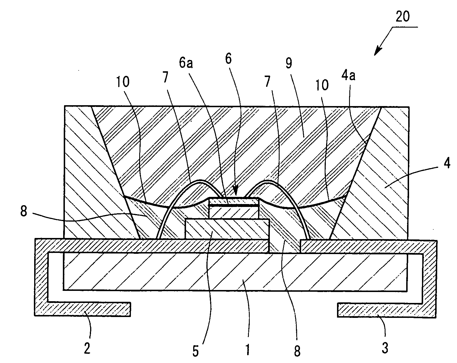
[0034]FIG. 1 is a sectional view of a semiconductor light-emitting device 20 according to a first embodiment of the present invention. The semiconductor light-emitting device 20 includes a light-emitting diode 6, prepared by growing a crystal of a Group-III nitride compound semiconductor on a sapphire substrate, emitting blue light with a peak emission wavelength of 460 nm. The light-emitting diode 6 is soldered on a submount 5 in a face-up manner. The submount 5 is made of aluminum (Al) and is fixed to a first lead electrode 2. The light-emitting diode 6 has electrodes connected to the first lead electrode 2 and a second lead electrode 3 with bonding wires 7. The first and second lead electrode 2 and 3 are made of metal and are fixed on an insulating resin substrate 1. A resin case 4 coated with a reflecting agent 4a is fixed on the first and second lead electrode 2 and 3. The inner wall of the resin case 4 is inclined, because the extraction efficiency of output light is enhanced ...

first modification

[0051]In the first embodiment, the deposition layer 10 has a thickness equal to that of a one- or two-particle layer. The deposition layer 10 may have a thickness equal to that of a one-particle to five-particle layer depending on target chromaticity. The collision frequency of a photon with one of the phosphor particles or light diffuser particles is preferably zero or one in view of light shift and / or luminous efficiency and therefore the deposition layer 10 preferably has a thickness equal to that of such a one- or two-particle layer. In order to increase the collision frequency thereof, the deposition layer 10 may have a thickness equal to that of such a one-particle to five-particle layer depending on target chromaticity. Even under such a design condition, color shift can be effectively prevented in such a manner that the deposition layer 10 is uniformly formed.

second modification

[0052]In the semiconductor light-emitting device 20 according to the first embodiment, the liquid second epoxy resin which is not cured yet and which is used to form the secondary sealing member 9, may contain particles of a light diffuser instead of or in addition to the phosphor particles. In this case, the deposition layer 10 contains the light diffuser particles and / or the phosphor particles and can be formed densely and uniformly so as to have an extremely small thickness; hence, the deposition layer 10 is effective in achieving a sufficient light-diffusing effect. This configuration is effective in preventing a reduction in luminous efficiency due to unnecessary scattering.


PUM


Abstract

A semiconductor light-emitting device in which a light-emitting diode including a light-emitting layer is placed directly on the bottom of a cup-shaped case or placed above the case bottom with a submount disposed therebetween includes a transparent primary sealing member that seals a side region, located under the light-emitting layer, surrounding the light-emitting diode that is fixed in the case; a transparent secondary sealing member disposed on the primary sealing member; and a uniform deposition layer formed by depositing phosphor particles or light diffuser particles contained in a material for forming the secondary sealing member. The phosphor particles or the light diffuser particles are deposited on the upper surface of the light-emitting diode and the upper surface of the primary sealing member to form a uniform layer that is as thin as a one-particle to five-particle layer.

Description

BACKGROUND OF THE INVENTION[0001]1. Field of the Invention[0002]The present invention relates to a semiconductor light-emitting device in which a light-emitting diode is placed directly on the bottom of a cup-shaped case or placed above the case bottom with a submount disposed therebetween and also relates to a method for manufacturing the semiconductor light-emitting device. The present invention particularly relates to the arrangement of particles of a phosphor or a light diffuser.[0003]2. Description of the Related Art[0004]The following documents disclose semiconductor light-emitting devices in which light-emitting diodes are placed on the bottoms of cup-shaped cases and which contain phosphors: Japanese Unexamined Patent Application Publication Nos. 2002-222996, 2004-111882, and 2006-93540. The semiconductor light-emitting devices are characterized in that the position (height) of each phosphor is limited to a certain level in such a manner that a sealant is packed in each case...

Claims


Application Information

Patent Timeline
IPC IPC(8): H01J1/62H01J9/02H01L33/50H01L33/32H01L33/54H01L33/56H01L33/60H01L33/62
CPCH01L33/508H01L33/54H01L2933/0091H01L2224/48247H01L2224/48091H01L2924/00014
Inventor HARUNA, TAKAONAMIKI, AKIO
Owner TOYODA GOSEI CO LTD
Why Eureka
Try Eureka