Method for preparing two-dimensional photonic crystal structure GaN (gallium nitride) based LED (light emitting diode)

A two-dimensional photonic crystal and photonic crystal technology, applied in the field of optoelectronics, can solve problems such as uneven photonic crystal graphics and poor photonic crystal graphics, and achieve the effects of convenient graphics transfer, increased etching selection ratio, and improved light extraction efficiency

Inactive Publication Date: 2011-10-12
HUAZHONG UNIV OF SCI & TECH
View PDF1 Cites 44 Cited by
  • Summary
  • Abstract
  • Description
  • Claims
  • Application Information

AI Technical Summary

Problems solved by technology

After etching, the photonic crystal pattern is poor, some areas have photonic crystal pattern, and some places have no photonic crystal pattern, and the photonic crystal pattern is not uniform

Method used


Image

  • Method for preparing two-dimensional photonic crystal structure GaN (gallium nitride) based LED (light emitting diode)
  • Method for preparing two-dimensional photonic crystal structure GaN (gallium nitride) based LED (light emitting diode)
  • Method for preparing two-dimensional photonic crystal structure GaN (gallium nitride) based LED (light emitting diode)

Examples


Embodiment example 1

[0050] A method for preparing a GaN-based LED with a two-dimensional photonic crystal structure, comprising the steps of:

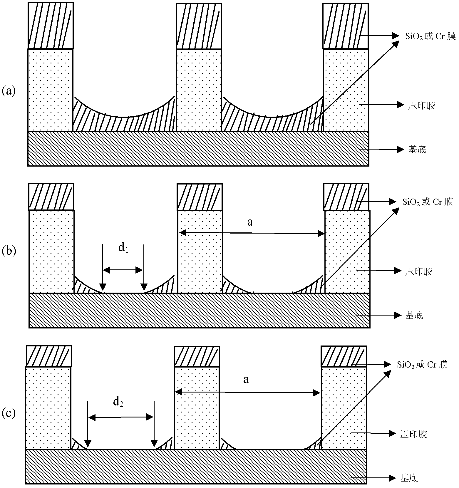
[0051] 1. Prepare a hard template containing a two-dimensional photonic crystal pattern, and perform anti-sticking treatment on the hard template. Nanoimprint hard templates can include silicon templates; porous alumina (AAO) templates, and silicon-based porous alumina (AAO) templates.

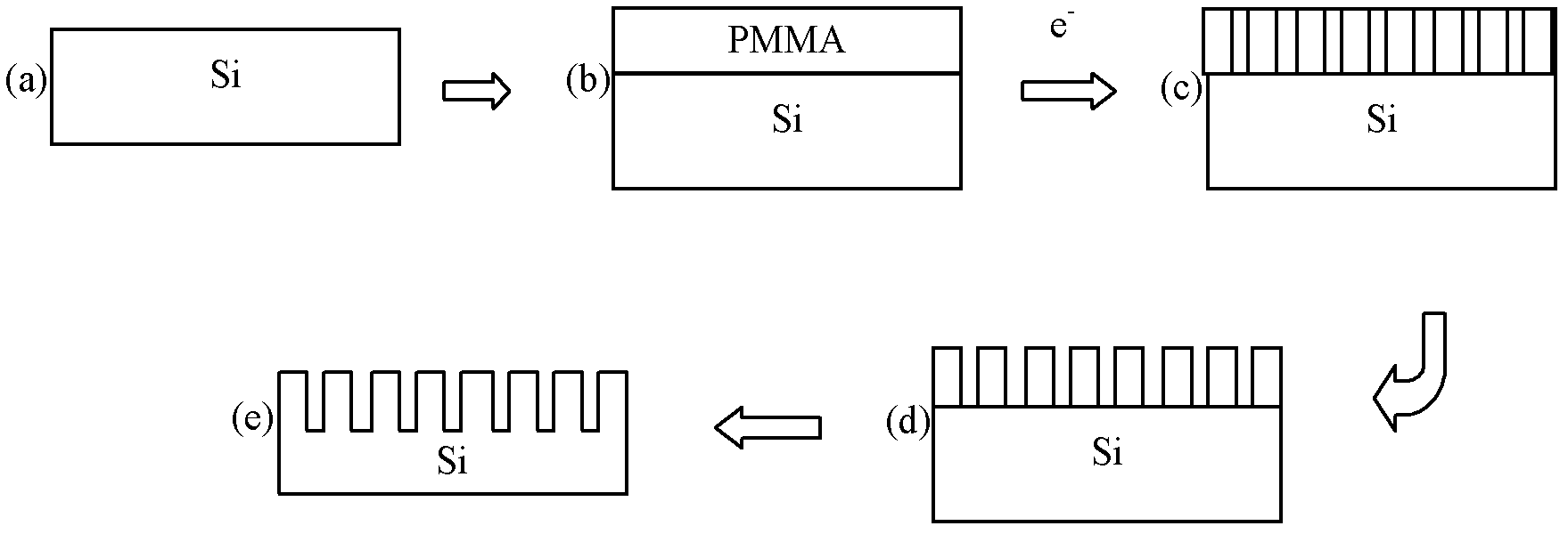
[0052] Among them, the silicon template can be prepared through the following process: clean the silicon wafer and dry it; then apply a layer of PMMA glue; carry out electron beam exposure according to the design pattern; remove the exposed PMMA glue by developing; use PMMA glue as the Mask etching Si to obtain the Si template of the desired pattern, such as image 3 (a)-3(e).

[0053] The AAO template can be prepared by the following process: put pure aluminum (above 99.99%) into a 0.1-0.5mol / L mixed solution of oxalic acid, sulfuric acid or phosphoric acid, and use a ...

Embodiment 2

[0072] The difference between this embodiment and Embodiment 1 is that the target wafer is a GaN epitaxial wafer growing an ITO layer, such as Figure 12 shown. Specific steps are as follows:

[0073] 1. The preparation of the nanoimprint hard template is the same as the first step of Example 1.

[0074] 2. The preparation of the soft template for nanoimprinting is the same as the second step of Example 1.

[0075] 3. Preparation of target slices

[0076] Clean the sapphire substrate (1) first, then deposit the buffer layer (2) and the semiconductor epitaxial stack on the substrate (1) by metal organic chemical vapor deposition (MOVCD), molecular beam epitaxy (MBE) and other semiconductor epitaxial growth methods. The layer structure is the target sheet; the semiconductor epitaxial layer at least includes an N-type layer (3), a light-emitting layer (4), a P-type layer (5) and an ITO layer (6) from bottom to top; the light-emitting layer 4 usually has quantum Well structure...

Embodiment 3

[0087] The difference between this embodiment and Embodiment 1 is that the target sheet in this implementation is to adopt a sapphire substrate sheet, such as Figure 13 shown. Specific steps are as follows:

[0088] 1. The preparation of the nanoimprint hard template is the same as the first step of Example 1.

[0089] 2. The preparation of the soft template for nanoimprinting is the same as the second step of Example 1.

[0090] 3. Preparation of target slices

[0091] Prepare the sapphire substrate 1 and clean it.

[0092] 4. Uniform glue: Spin coat a layer of STU UV glue on the target sheet, first rotate at a speed of 500rpm for 5s, so that the hot-pressed glue is evenly spread on the SiO2 surface, and then rotate at a speed of 3000rpm for 45s to shake off the excess Ultraviolet glue will be thinned and homogenized; and then baked on a hot plate at 95°C for 3mins to obtain the target sheet A, such as Figure 8 as shown in (b);

[0093] 5. Embossing: The above soft temp...


PUM

PropertyMeasurementUnit
thicknessaaaaaaaaaa
thicknessaaaaaaaaaa
thicknessaaaaaaaaaa

Abstract

The invention discloses a method for preparing a two-dimensional photonic crystal structure GaN (gallium nitride) based LED (light emitting diode). The method comprises: firstly, spinning a layer of ultraviolet optical resist on a target; copying the two-dimensional photonic crystal structure of a template to the surface of the optical resist by utilizing ultraviolet soft nanoimprinting, and etching to remove the residual resist; evaporating a layer of SiO2 or Cr film on a photonic crystal ultraviolet resist, thus a photonic crystal image is obtained on a target sheet through etching; and theobtained GaN is subjected to removing of photoresist, cleaning and drying, thus a photonic crystal target sheet is obtained, and carrying out subsequent process treatment on the obtained target sheet, thus the manufacturing of a device is finished, and the photonic crystal GaN based LED with high light extracting efficiency is obtained. Through the method provided by the invention, the selection ratio of etching can be improved, the duty ratio of the photonic crystal can be regulated in a certain range, the uneven problem of the surface of the LED chip can be overcome, the photonic crystal image can be prepared better through the nanoimprinting technology, and the method is suitable for the preparation of the GaN based photonic crystal LED in industrial production.

Description

technical field [0001] The invention relates to GaN-based light-emitting diodes (LEDs), more specifically, to a method for preparing GaN-based LEDs based on nanoimprint technology, and belongs to the field of optoelectronic technology. Background technique [0002] Since the invention of GaN-based semiconductor light-emitting diode (LED), it has been widely used in lighting, display screen, communication equipment and other fields. With the increasing emphasis on energy-saving demand in the world, LED lighting technology has attracted people's attention due to its high energy-saving potential. But because GaN has a high refractive index (n≈2.5) coefficient, only a small part (about 4%) of light can escape from the GaN-based epitaxial surface. At present, the light extraction efficiency of high-power GaN-based LEDs is low, and more work is needed. In order to improve the light extraction efficiency of LEDs and obtain high-efficiency light output, various technologies have b...

Claims


Application Information

Patent Timeline
Patent Type & Authority Applications(China)
IPC IPC(8): H01L33/00G03F7/00
Inventor 吴小锋徐智谋刘文孙堂友李程程赵文宁王双保
Owner HUAZHONG UNIV OF SCI & TECH
Why Eureka
Try Eureka