[0007]Provided are methods and systems for
dry transfer printing of semiconductors and semiconductor elements by shear offset. Shear
offset printing systems permit higher
delamination rates to be achieved during transfer printing without sacrificing printing yield or accuracy, compared to conventional techniques that do not apply a shear offset. Accordingly, methods and systems presented herein provide faster and more reliable transfer printing, thereby reducing
processing time and increasing printing efficiency.
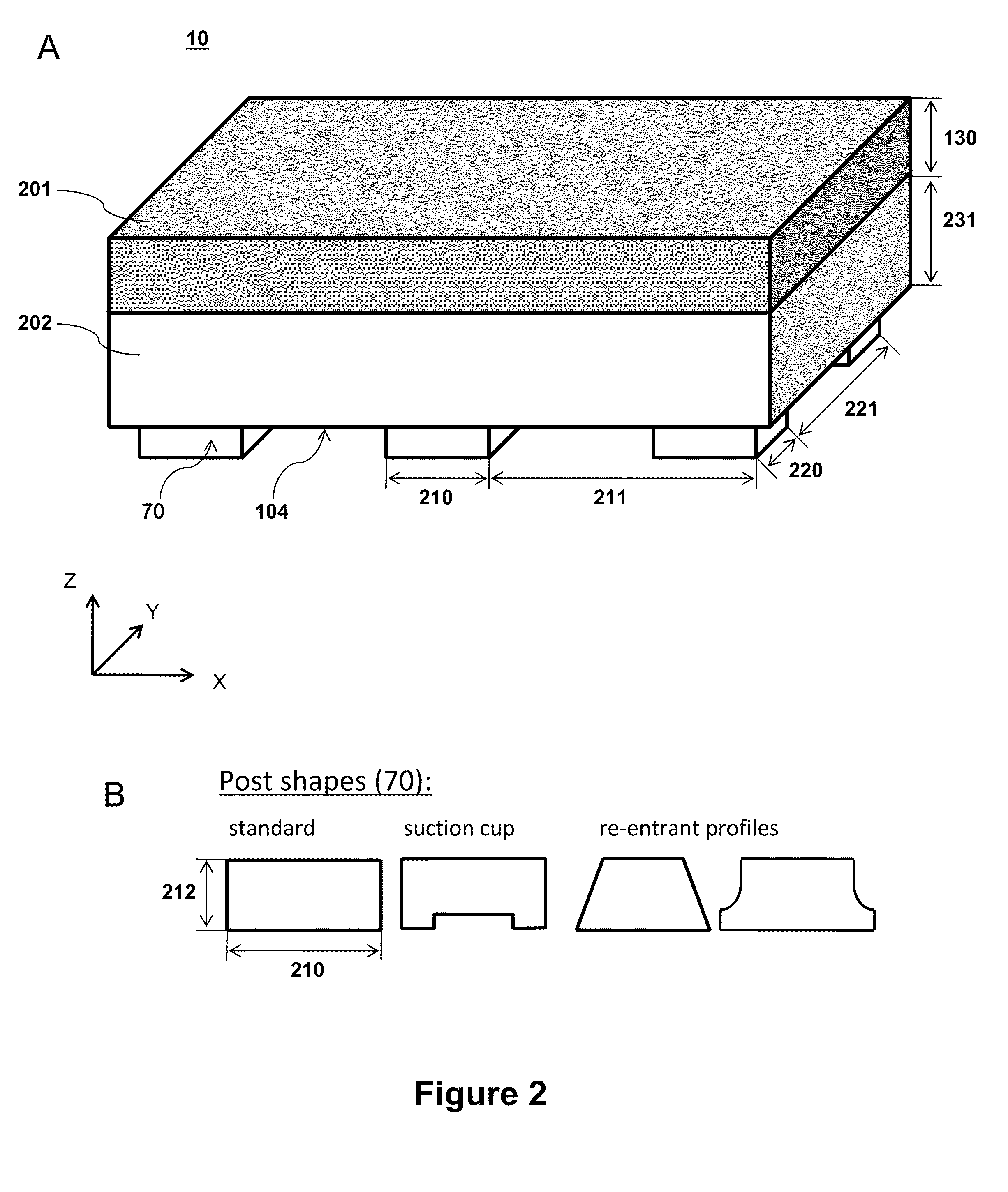
[0013]In an embodiment, any of the stamps used in any of the processes or devices disclosed herein may be a composite stamp. In an aspect, the elastomeric stamp has an elastomeric layer with a top surface that is opposite the transfer surface and a rigid backing layer having a bottom surface, wherein the bottom surface is positioned adjacent to the elastomeric layer top surface. Such elastomeric stamps having a rigid backing layer are advantageous for transferring applied pressure and motion (e.g., vertical and / or horizontal) to the interface between the transfer surface and the inked semiconductor element and / or the receiving
substrate surface. For example, air pressure applied to the rigid backing can be uniformly transmitted to the active printing area. In another aspect, the elastomeric stamp also has a reinforcement layer operably connected to the rigid backing layer, the reinforcement layer having an opening that vertically coincides with at least a portion of the relief features on the transfer surface.
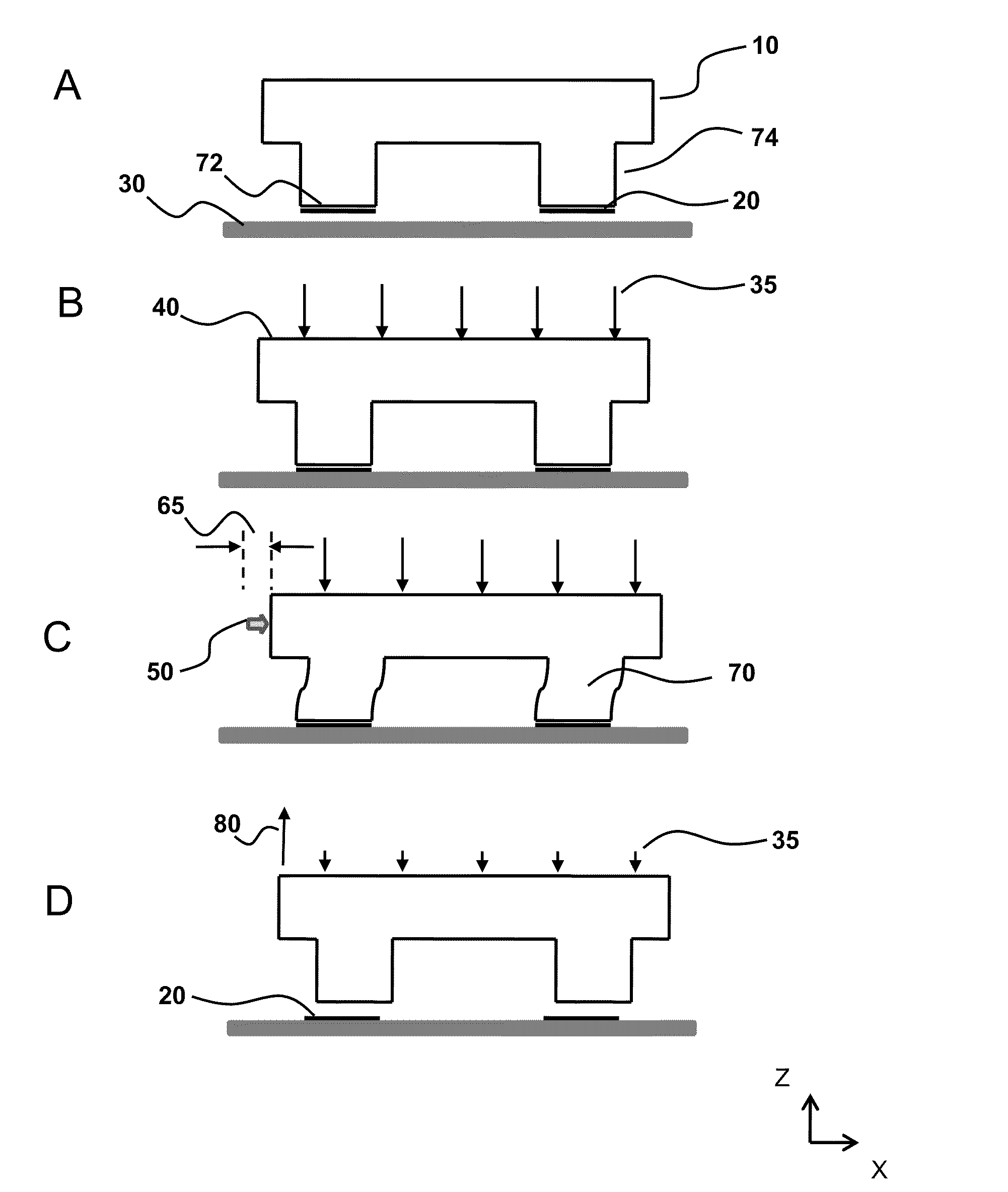
[0017]In an embodiment the relief features comprise a plurality of posts. The posts can help facilitate semiconductor element lift-off from a donor surface and / or semiconductor element transfer from the stamp to the receiving surface. In an aspect of this embodiment, the plurality of posts have a contacting
area fraction on the transfer surface selected from a range that is greater than 1% and less than 25%. “Contacting
area fraction” refers to the percentage of surface
area coverage by the posts over the printable surface area region. In an aspect where the relief features comprise a plurality of populations, the relief features may further comprise a plurality of stabilization features interspersed between the posts, wherein said stabilization features have a contacting area that is less than the contacting area of the posts.
[0023]For aspects where air pressure is applied to at least partially establish said conformal contact and the stamp is vertically separated from the receiving surface, each of the air pressure and vertical separation rate may vary over time during the delamination cycle. For example, in embodiments where the delamination cycle is divided into at least two time intervals, with the first interval is before the second interval, and does not substantially overlap, the air pressure may vary over the first time interval while the vertical separation is maintained constant over this first time interval. In contrast, during the second time interval the air pressure may be maintained constant while the vertical separation increases during this second time interval. In this embodiment, selection of the pressure and separation distance with respect to time is an optimization step that helps facilitate a constant delamination rate over the delamination cycle, such a delamination rate that deviates less than or equal to a user-specified deviation, such as less than or equal to 5% from an average delamination rate over the first and second time intervals.
[0025]In an embodiment, the device supports a reinforced composite stamp having a deformable layer with an internal surface and an external surface positioned opposite the internal surface, the external surface of the deformable layer having a plurality of relief features. A rigid support layer is connected to the internal surface of the deformable layer, wherein the rigid support layer has a bottom surface and a top surface positioned opposite the bottom surface, wherein the bottom surface is positioned
proximate to the internal surface of the deformable layer. A reinforcement layer is operably connected to the rigid support layer, the reinforcement layer having an opening that vertically coincides with at least a portion of the relief features of the external surface of the deformable layer. In an embodiment, the composite stamp is supported by a vertical section that operably connects a mounting
flange to the deformable layer external surface. A transfer printing tool head having a receiving surface connects the mounting
flange top surface. An
actuator is operably connected to the mounting
flange or the transfer printing tool head for generating a horizontal displacement between the deformable layer internal surface and the receiving surface. Accordingly, the
actuator may displace the stamp or the receiving substrate, thereby achieving offset between the stamp and the receiving substrate.

