Semiconductor light-emitting device and method for fabricating the same

a technology of semiconductors and light-emitting devices, which is applied in the direction of semiconductor devices, basic electric elements, electrical equipment, etc., can solve the problems of difficult formation of ohmic electrodes, damage to p-type gan layers, and weak light-radiation pattern of led chips, so as to improve light-extraction efficiency and improve light-extraction efficiency. , the effect of high light-extraction efficiency

Inactive Publication Date: 2005-07-28
PANASONIC CORP
View PDF13 Cites 44 Cited by
  • Summary
  • Abstract
  • Description
  • Claims
  • Application Information

AI Technical Summary

Benefits of technology

[0013] With the foregoing in mind, an object of the present invention is to provide a semiconductor light-emitting device having a high light-extraction efficiency and a good radiation pattern without employing fine lithography technique and dry etching technique.
[0054] As is apparent from the above, with the present invention, the semiconductor layer having the surface serving as the light-extraction surface is made porous, whereby air gaps are formed randomly in the semiconductor layer. This improves the light-extraction efficiency of the device without generating any specific radiation pattern resulting from interference between diffracted lights. Moreover, the semiconductor layer can be made porous by wet etching. This eliminates a problem of damages induced by dry etching. Furthermore, the wavelength of the optical absorption edge of the semiconductor layer made porous shifts to shorter wavelength than that before the semiconductor layer is made porous. This reduces absorption of light emitted from the active layer, whereby the light-extraction efficiency of the device can be further improved. Moreover, it is unnecessary to use a fine photolithography technique for fabrication of the device. This enhances the fabrication yield.

Problems solved by technology

However, in the conventional technique described above, the light-extraction surface is formed with the regular projections and depressions, which causes a practical problem that a radiation pattern of light radiated from the LED chip is strengthened in specific directions by interference between diffracted lights.
Further, since dry etching is used to form the projections and depressions in the p-type GaN layer serving as the light-extraction surface, the p-type GaN layer is damaged.
This causes a problem that an ohmic electrode is difficult to form on the p-type GaN layer and a problem that light is absorbed into deep levels created in the p-type GaN layer.
Moreover, if light emitted from the active layer has a short wavelength, light absorption into the p-type GaN layer cannot be ignored.
However, if the conventional technique described above is employed in this case, the following problems arise.
First, since materials having large band gap energies generally have strong bonds and are firm, such materials are difficult to etch to form projections and depressions.
Second, on a layer made of the material having a large bad gap energy, formation of an ohmic electrode is further difficult.
This causes a problem of a decrease in the yield of the chip.

Method used


Image

  • Semiconductor light-emitting device and method for fabricating the same
  • Semiconductor light-emitting device and method for fabricating the same
  • Semiconductor light-emitting device and method for fabricating the same

Examples


first embodiment

MODIFICATION OF FIRST EMBODIMENT

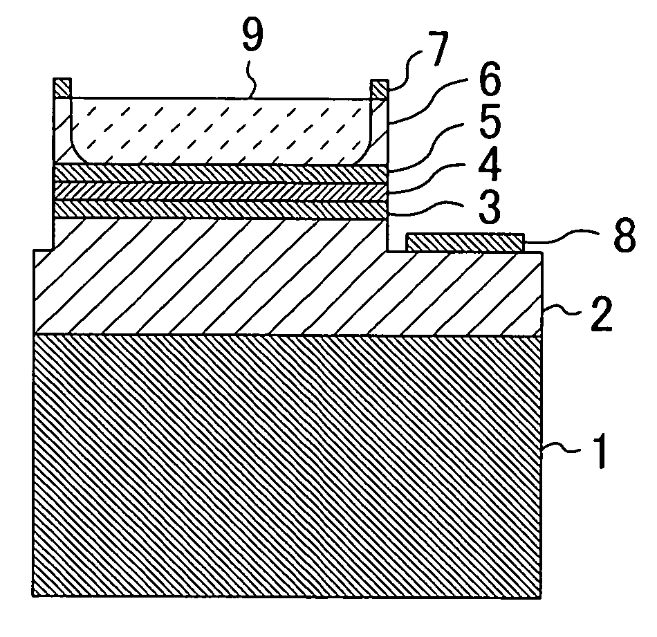
[0087] A semiconductor light-emitting device and a method for fabricating the device according to a modification of the first embodiment of the present invention will be described below with reference to the accompanying drawings. This modification differs from the first embodiment in the cross-sectional construction of the porous structure 9 in the p-type GaN contact layer 6. That is to say, the basic construction, other than the porous structure 9, of the semiconductor light-emitting device according to this modification is similar to that of the device according to the first embodiment shown in FIGS. 1A and 1B.

[0088]FIG. 6 is a view schematically showing the cross-sectional structure of the porous structure 9 of the p-type GaN contact layer 6 in the semiconductor light-emitting device according to this modification.

[0089] The method for fabricating a semiconductor light-emitting device according to this modification is as follows. First, using an...

second embodiment

[0102] A semiconductor light-emitting device and a method for fabricating the device according to a second embodiment of the present invention will be described below with reference to the accompanying drawings.

[0103]FIG. 7 is a view showing the cross-sectional structure of the semiconductor light-emitting device according to the second embodiment. The semiconductor light-emitting device according to the second embodiment differs from the device according to the first embodiment (see FIGS. 1A and 1B) in that as shown in FIG. 7, not the p-type GaN contact layer 6 but a p-type AlGaN contact layer 10 with a gradient composition is formed of which the Al content continuously decreases, for example, from about 10 to 0% from the substrate side toward the surface side. All components other than that are identical to those in the first embodiment including the fabrication method thereof FIG. 8 is a view schematically showing the cross-sectional structure of a porous structure 9 of the p-ty...

third embodiment

[0106] A semiconductor light-emitting device and a method for fabricating the device according to a third embodiment of the present invention will be described below with reference to the accompanying drawings. The semiconductor light-emitting device according to the third embodiment differs from the device according to the second embodiment (see FIGS. 7 and 8) in the detail construction of a porous structure 9 in a p-type AlGaN contact layer 10 with a gradient composition. That is to say, the device structure in the third embodiment other than this detail construction is identical to that in the second embodiment.

[0107]FIG. 9 is a view schematically showing the cross-sectional structure of the porous structure 9 of the p-type AlGaN contact layer 10 with a gradient composition included in the semiconductor light-emitting device according to the third embodiment.

[0108] Referring to FIG. 9, in the third embodiment, on the semiconductor surface of the p-type AlGaN contact layer 10 wi...


PUM


Abstract

In a semiconductor light-emitting device formed by stacking a plurality of semiconductor layers including an active layer, at least a portion of a semiconductor layer of the plurality of semiconductor layers is made porous. The semiconductor layer made porous has a surface serving as a light-extraction surface for extracting light emitted from the active layer.

Description

CROSS-REFERENCE TO RELATED APPLICATIONS [0001] This application claims priority under 35 U.S.C. § 119 on Patent Application No. 2004-019410 filed in Japan on Jan. 28, 2004, the entire contents of which are hereby incorporated by reference. BACKGROUND OF THE INVENTION [0002] (a) Fields of the Invention [0003] The present invention relates to semiconductor light-emitting devices, typified by light-emitting diodes (referred hereinafter to as LEDs), usable as various types of indicators, backlights for liquid-crystal displays, light sources for solid illuminations, and the like. [0004] (b) Description of Related Art [0005] In recent years, LEDs have been growingly sophisticated in functionality and application areas of the LEDs have been increasingly widened rapidly. In particular, with the advent of nitride-based compound semiconductors typified by gallium nitride (referred hereinafter to as GaN), LEDs covering a wide range from ultraviolet to all visible regions have come to be realiz...

Claims


Application Information

Patent Timeline
Patent Type & Authority Applications(United States)
IPC IPC(8): H01L21/00H01L33/16H01L33/22
CPCH01L33/22H01L33/16
Inventor YURI, MASAAKI
Owner PANASONIC CORP
Why Eureka
Try Eureka