Nitride semiconductor light emitting element

Active Publication Date: 2010-07-01
SHARP KK
View PDF5 Cites 48 Cited by
  • Summary
  • Abstract
  • Description
  • Claims
  • Application Information

AI Technical Summary

Benefits of technology

[0017]According to the present invention, since the recess regions or rise regions each having the shape of a polygon having an interior angle of 180° or greater is formed on the substrate, there are formed spaces at portions opposite to the portions each having the interior angle. In each of the spaces, an adjacent recess region or rise region is disposed. In this way, the recess regions and the rise regions can be formed in close proximity to one another on the substrate in high density.
[0018]Light emitted from the light emitting

Problems solved by technology

Even though recesses and rises are formed on the substrate or the p type contact layer as in each of the above-described semiconductor light emitting elements of Japanese Patent Laying-Open No. 2005-317931, Japanese Patent Laying-Open No. 2008-153634, Japanese Patent Laying-Open No. 2005-

Method used


Image

  • Nitride semiconductor light emitting element
  • Nitride semiconductor light emitting element
  • Nitride semiconductor light emitting element

Examples


experimental example 1

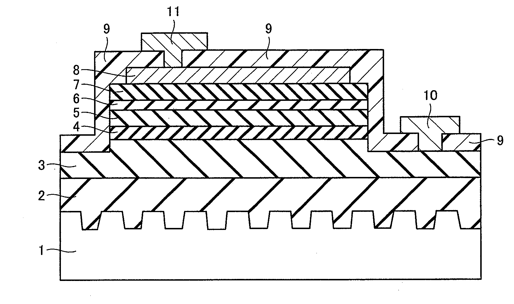
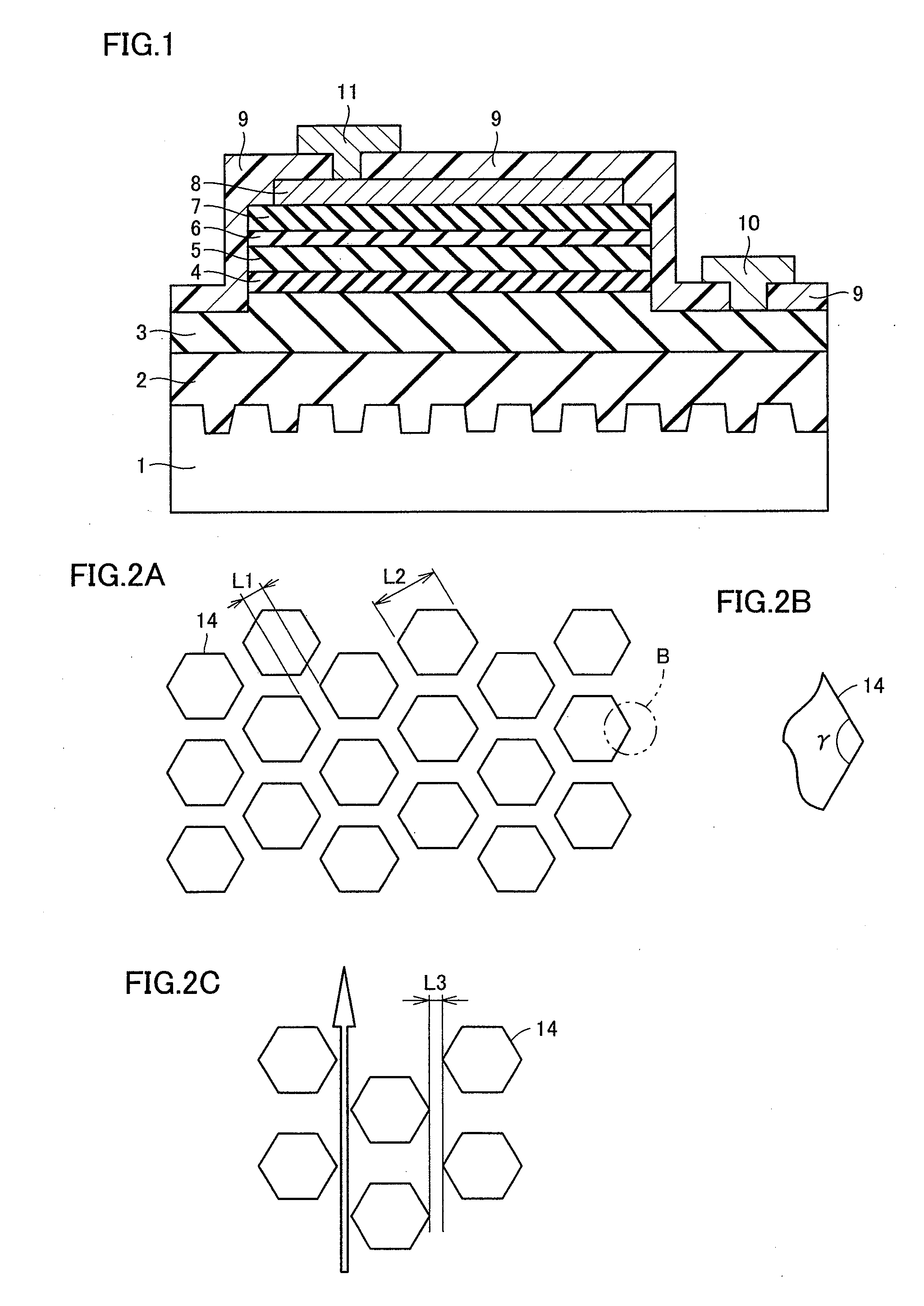
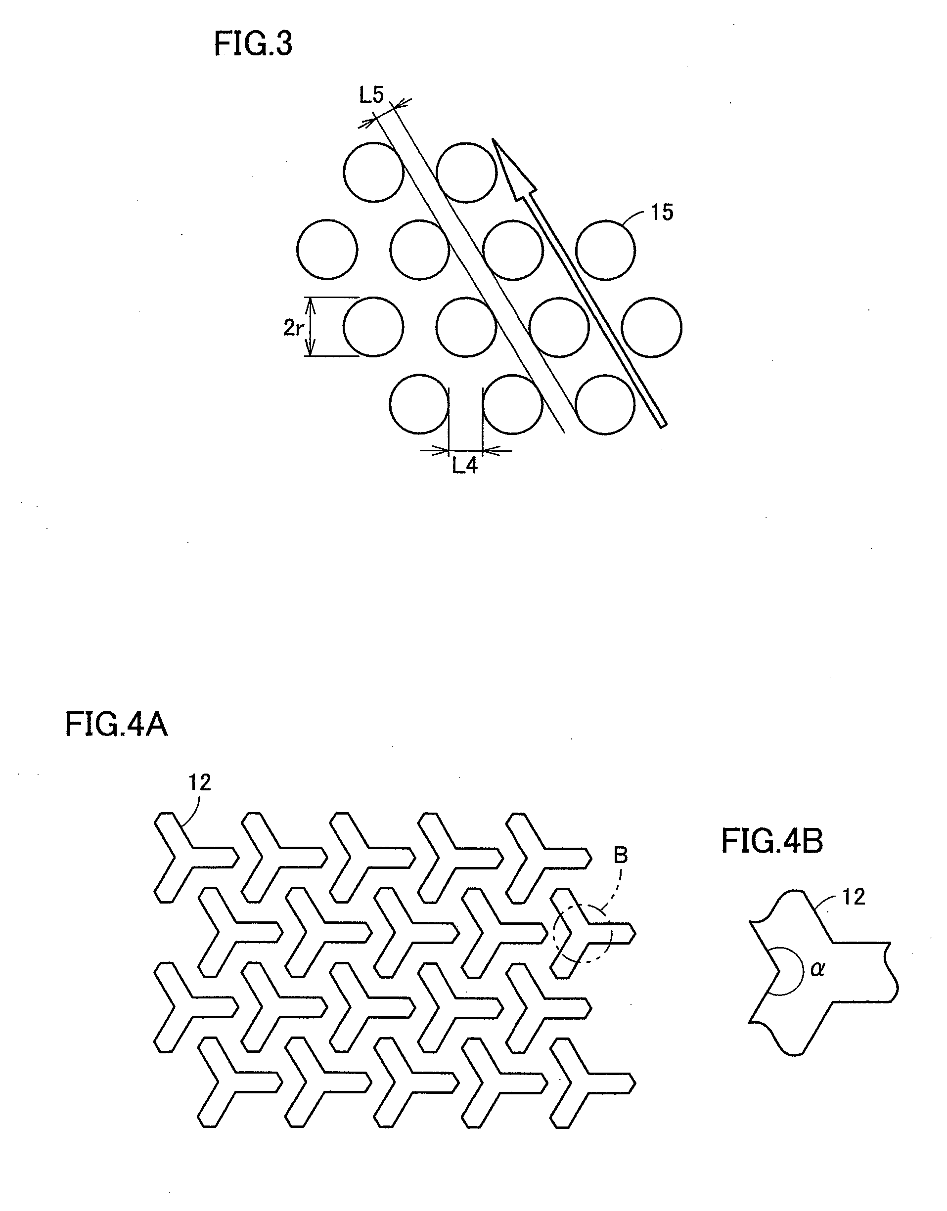
[0102]The following describes results of measuring outputs of light emitting elements having the five patterns of rise regions or recess regions formed on the upper surface of light transmitting substrate 1, i.e., the rise regions or recess regions of FIGS. 2A, 2C, 3, 4A, and 5A. As to the shapes shown in FIGS. 4A, 5A, when the narrowest portion of each of the rise regions had a width of 1.5 μm and the narrowest portion of each of the recess regions had a width of 1.5 μm, the outputs of the corresponding light emitting elements were 30 mW at a voltage of 3.1 V.

[0103]As to the shape shown in FIG. 2A, with L1=1 μm and L2=3.5 μm, the output of the light emitting element was 29 mW at a voltage of 3.1 V. As to the shape shown in FIG. 3, with L4=1μm and r=5 μm, the output of the light emitting element was 27 mW at a voltage of 3.1V. As to the shape shown in FIG. 2C, the output of the light emitting element was approximately 20-25 mW at a voltage of 3.1V.

[0104]As such, it can be recognized...

experimental example 2

[0107]The following describes a method for forming a nitride semiconductor light emitting element in which an AIN buffer layer 16 was formed, as well as a result of measuring its output.

[0108]First, as with experimental example 1, the recess and rise regions each having the shape shown in FIG. 4A or FIG. 5A were formed on the surface of light transmitting substrate 1. As light transmitting substrate 1, a sapphire substrate was used. Light transmitting substrate 1 was placed on a heater provided within a chamber of a DC magnetron sputtering device, in which voltage is applied through the DC-continuous method.

[0109]Light transmitting substrate 1 was placed thereon so that the c-plane of light transmitting substrate 1 faced the surface of an Al target and the shortest distance between the center of the surface of the Al target and the c-plane of light transmitting substrate 1 was 50 mm. In this state, light transmitting substrate 1 was heated to 500° C. by the heater. Thereafter, only ...


PUM


Abstract

In a nitride semiconductor light emitting element, a light transmitting substrate has an upper surface on which a nitride semiconductor layer including at least a light emitting layer is formed. On the upper surface of the light transmitting substrate, recess regions and rise regions are formed. One of each of the recess regions and each of the rise regions is formed by a polygon having at least one apex having an interior angle of 180° or greater when viewed in a planar view. The other of each of the recess regions and each of the rise regions is formed not to be connected to one another in a straight line when viewed in a planar view. A nitride semiconductor light emitting element having such a configuration has excellent light extraction efficiency and can be manufactured at a moderate cost.

Description

[0001]This nonprovisional application is based on Japanese Patent Application No. 2008-332308 filed on Dec. 26, 2008 and No. 2009-241053 filed on Oct. 20, 2009, with the Japan Patent Office, the entire contents of which are hereby incorporated by reference.BACKGROUND OF THE INVENTION[0002]1. Field of the Invention[0003]The present invention relates to a nitride semiconductor light emitting element, in particular, to a nitride semiconductor light emitting element with a light transmitting substrate having an upper surface provided with recesses and rises.[0004]2. Description of the Background Art[0005]Conventionally, for nitride semiconductor light emitting elements, sapphire (Al2O3) substrates, SiC substrates, GaN substrates, spinel (MgAl2O4) substrates, and the like have been used. Such nitride semiconductor light emitting elements are different from other compound semiconductor light emitting elements in that they employ the above-described substrates, which have a light transmitt...

Claims


Application Information

Patent Timeline
IPC IPC(8): H01L33/00
CPCH01L21/0242H01L21/0243H01L21/02458H01L21/0254H01L33/007H01L33/22
Inventor FUDETA, MAYUKO
Owner SHARP KK
Why Eureka
Try Eureka