

Structure for confining the switching current in phase memory (PCM) cells
a phase memory and structure technology, applied in the phase field, can solve the problems of difficult creation of phase change memory cells with power demands that are compatible with current state-of-the-art integrated circuit design rules, and achieve the effect of limiting heat dissipation
- Summary
- Abstract
- Description
- Claims
- Application Information
AI Technical Summary
Benefits of technology
Problems solved by technology
Method used
Image

Examples
Embodiment Construction
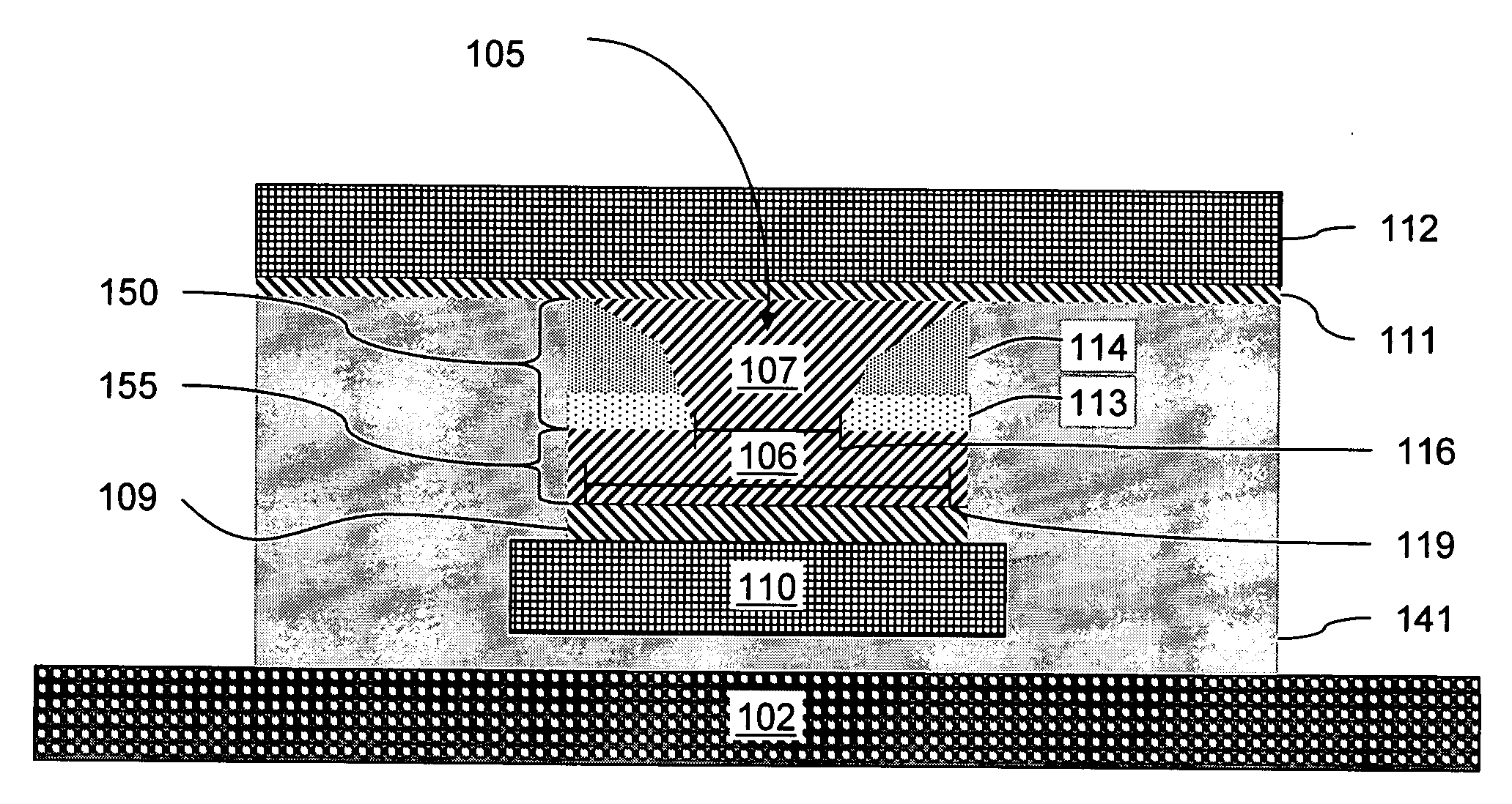
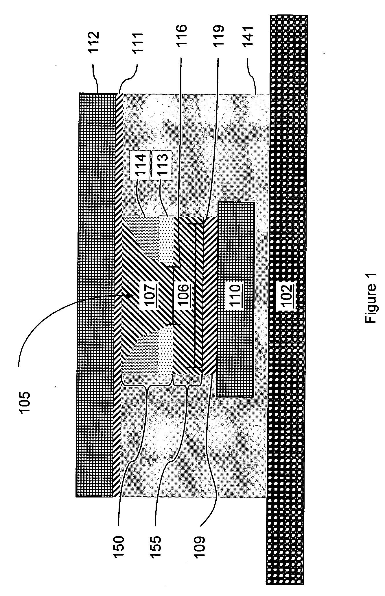
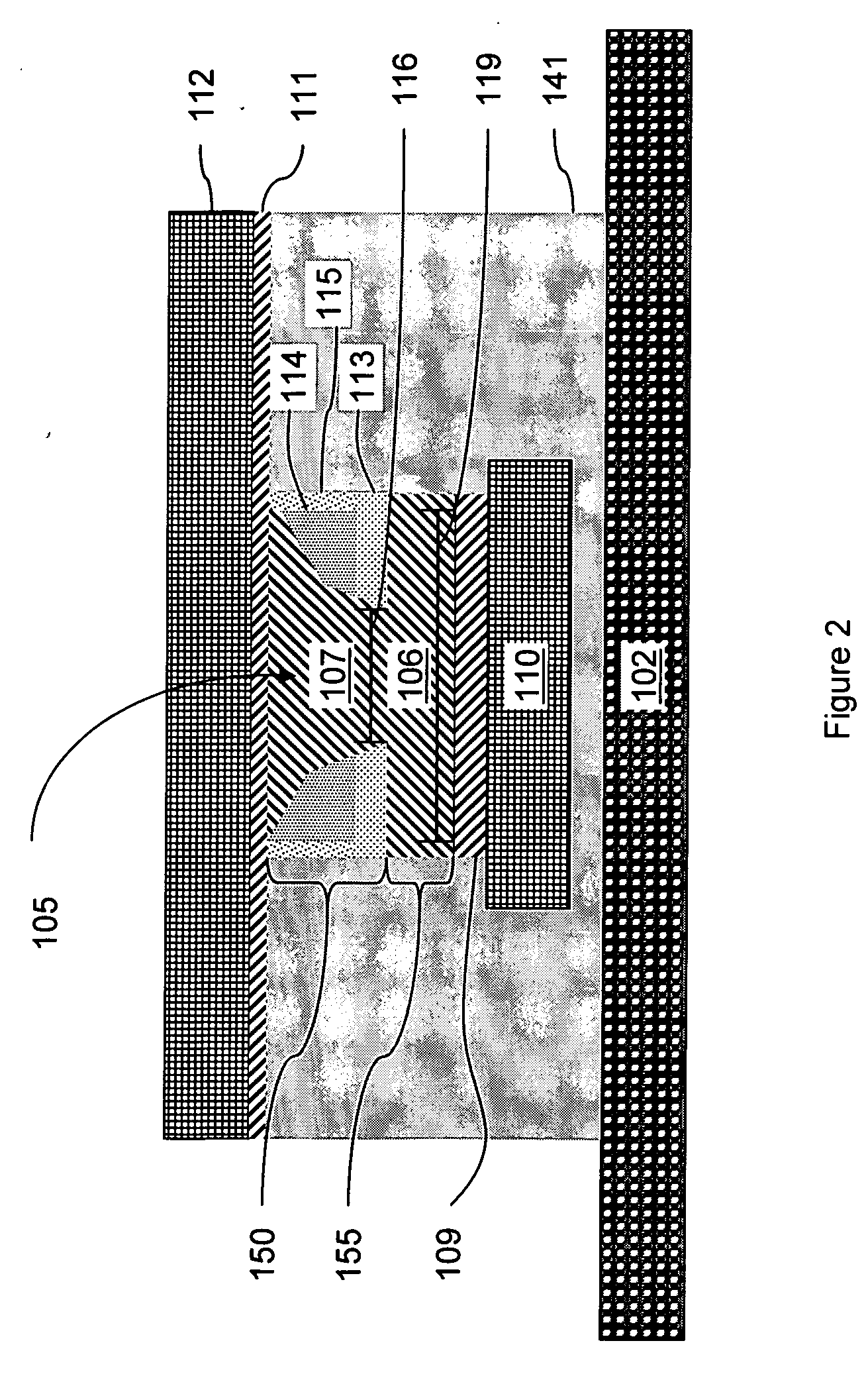
[0021] The present invention and the various features and advantageous details thereof are explained more fully with reference to the non-limiting embodiments that are illustrated in the accompanying drawings and detailed in the following description. It should be noted that the features illustrated in the drawings are not necessarily drawn to scale. Descriptions of well-known components and processing techniques are omitted so as to not unnecessarily obscure the present invention. The examples used herein are intended merely to facilitate an understanding of ways in which the invention may be practiced and to further enable those of skill in the art to practice the invention. Accordingly, the examples should not be construed as limiting the scope of the invention. As discussed above, the availability of binary chalcogenide alloys such as doped SbTe and ternary chalcogenide alloys such as those composed by Germanium, Antimony and Tellurium (e.g., Ge2Sb2Te5 (GST)), and progress in li...
PUM
 Abstract
Description
Claims
Application Information