Method for forming insulation film

a technology of insulation film and silicone polymer, applied in the field of semiconductor technology, can solve the problems of affecting high-speed operations, affecting the adhesion of silicon-containing materials, and reducing the thermal stability of fluorinated amorphous carbon film, and achieve the effect of reducing the total flow

Inactive Publication Date: 2008-04-08
ASM JAPAN
View PDF17 Cites 332 Cited by
  • Summary
  • Abstract
  • Description
  • Claims
  • Application Information

AI Technical Summary

Benefits of technology

[0029]Also, by reducing the distance between the electrodes, using low-frequency RF power mixed with high-frequency RF power, and / or using a reaction gas containing no oxygen-supplying gas and / or crosslinking gas, a silicon carbide film (Si—C based structure), not a low-k film (Si—O based structure), can be formed, and the film density can increase.
[0031]Conventional SiC has a relatively low dielectric constant but does not sufficiently block moisture penetration, whereas conventional SiCN or SiCO has a relatively high dielectric constant but can effectively block moisture penetration. This may be because the conventional SiC has a low density of 1.1-1.3 g / cm3 as compared with the conventional SiCN or SiCO having a density of 1.8-2.0 g / cm3. In an embodiment, the insulation film has as low a dielectric constant as that of SiC or lower than that of SiC, but the insulation film has as high Cu-diffusion blocking ability and as high dry etching selectivity against a low-k film as SiCN or SiCO (having a dielectric constant of 4.0 to 4.5) which are formed using 3 MS or 4 MS as a precursor gas. The insulation film according to an embodiment of the present invention has a high density and thus exhibits high etching-selectivity as compared with a low-k film (an etching selectivity against a low-k film may be in the range of 5-10) and also exhibits low Cu-penetration thickness (which may be 5-15 mu as measured under the Cu-diffusion blocking test). Thus, in an embodiment, the insulation film can effectively be used for memory devices.
[0032]Further, by adding an additive gas, elastic modulus of the insulation film can be improved. When the insulation film serves as a barrier film, preferably, the barrier film has compressive stress in view of wiring stress and adhesion to an Al layer.
[0033]Further, when the average temperature of the reaction (in an embodiment, the temperature of the susceptor) is controlled at −50° C. to 100° C. (−50° C. to 50° C. in an embodiment, 50° C. to 100° C. in another embodiment) during the plasma treatment, the insulation film can possess good filling property (padding property) so that even if a surface having holes or wiring grooves on which the insulation film is deposited has a high aspect ratio such as 1 / 3 to 1 / 10 (e.g., a Shallow Trench Isolation (STI) structure formed in a Si substrate) or a wiring pitch of 100 nm or less (e.g., 45 mn to 100 nm for an Al / low-k structure), the insulation film can fill in the holes or grooves without creating voids (as a low-k film or an oxide film). When the temperature is low, the precursor which is once vaporized when entering the reaction chamber becomes in an activated liquid state in the vicinity of a substrate surface, and thus the depositing film can exhibit excellent step coverage and filling property.
[0036]In an embodiment, by a combination of the above preliminary treatment for improving affinity between an underlying layer and an insulation film and the above deposition process using an additive gas a CxHyOz gas for reducing the viscosity of the reaction gas, the filling property or padding property of the insulation film (oxide film or low-k film) can significantly be improved.

Problems solved by technology

In these multi-layered structures, however, capacitance among individual wires hinders high speed operations.
First, the fluorinated amorphous carbon film has lower thermal stability (370° C.
), poor adhesion with silicon-containing materials and also lower mechanical strength.
The lower thermal stability leads to damage under high temperatures such as over 400° C. Poor adhesion may cause the film to peel off easily.
Further, the lower mechanical strength can jeopardize wiring materials.
As a result, the relative dielectric constant of the film cannot be reduced to a desired degree.
As a result, the source gas cannot stay in the reaction chamber for a sufficient length of time to cause polymerization in a vapor phase.
Further, the SOG insulation film of the spin-coat method has a problem in that the material cannot be applied onto the silicon substrate evenly and another problem in which a cure system after the coating process is costly.
However, copper tends to migrate or diffuse into the silica insulation films.
If SiC containing no impurities is used, the dielectric constant can be reduced, but the barrier film of SiC entails the moisture absorption problem.
However, wiring pitch or node becomes small (e.g., a wiring pitch of 45-100 nm), it is expected that low wiring delay times of Al wiring will be a problem.
Conventional low-k films do not have good padding ability.

Method used


Image

  • Method for forming insulation film
  • Method for forming insulation film
  • Method for forming insulation film

Examples


example 1

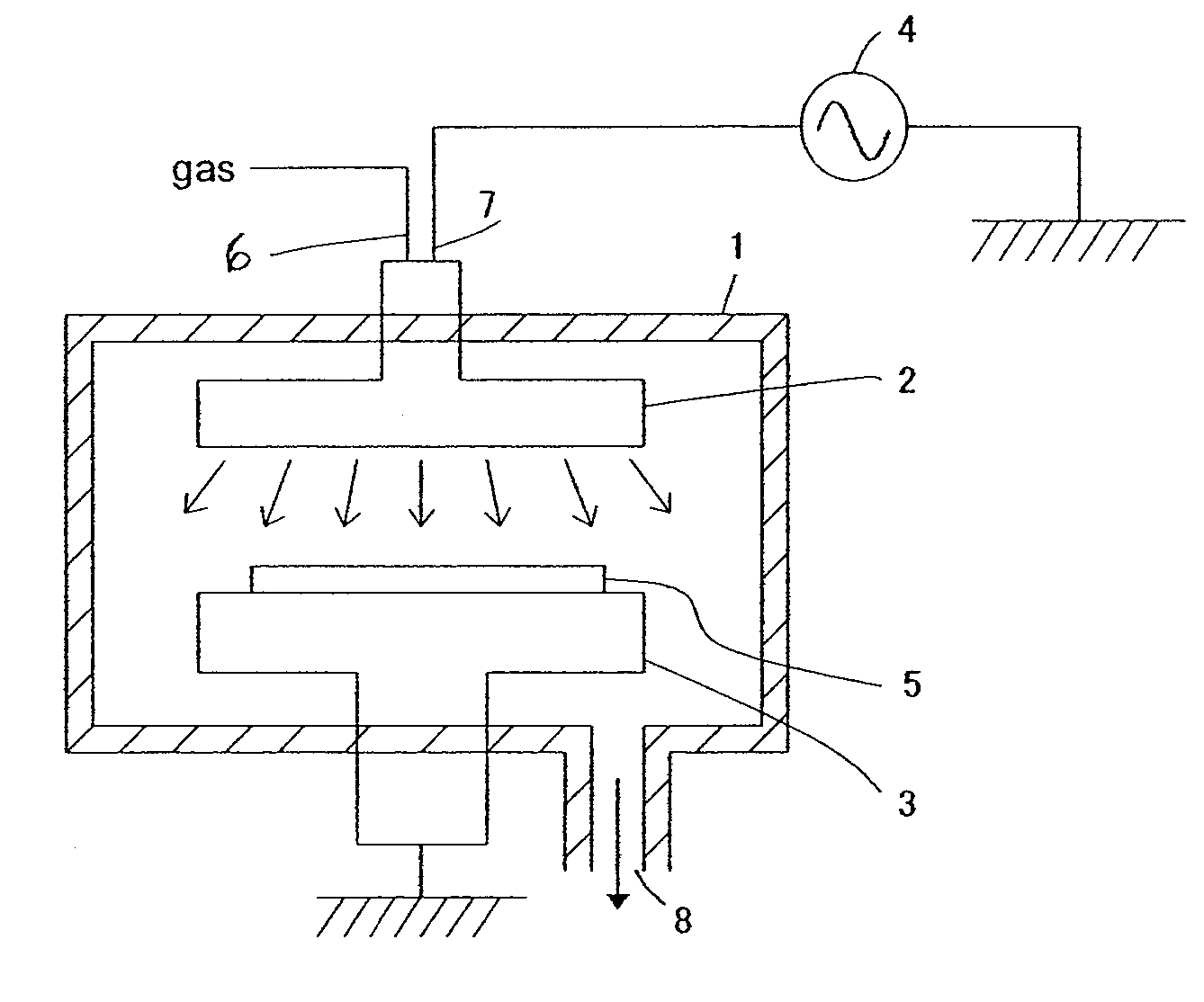
[0136]An insulation film was formed on a substrate using a plasma CVD apparatus shown in FIG. 1 under the following conditions, and the resultant thin film had the following properties:[0137]Susceptor temperature: 400° C.[0138]DM-DEOS (dimethyldiethoxysilane) flow rate: 100 sccm[0139]He flow rate: 70 sccm[0140]27 MHz RF applied: 1600 W[0141]Reactor pressure: 600 Pa[0142]Dielectric constant: 2.9[0143]Modulus: 20 GPa[0144]Film stress: 40 MPa (tensile)[0145]Space between the silicon substrate and the upper electrode: 0.024 m[0146]Residence time: 320 msec.

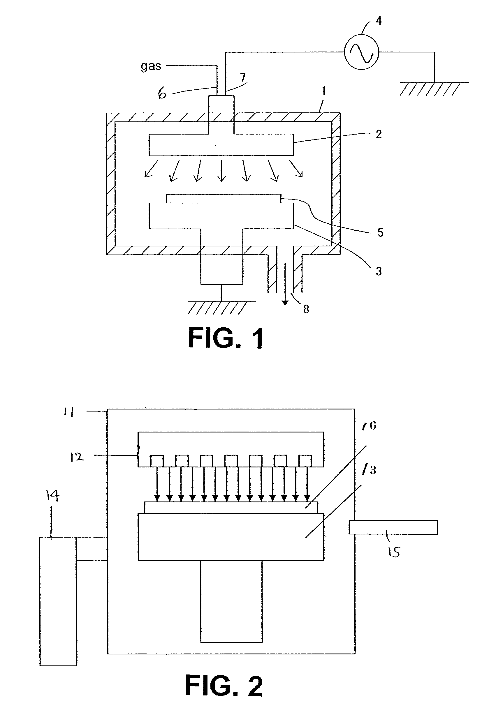
[0147]The thin film formed on the substrate was then cured using a curing apparatus shown in FIG. 2 under the following conditions, and the cured film had the following properties:[0148]UV curing process: Wavelength: 172 nm, 3-10 mW / cm2, Susceptor temperature: 300° C., N2: 5 SLM, Pressure: 45 Torr, Time: 70 sec.[0149]Dielectric constant: 3.0[0150]Film shrinkage: 5.3%[0151]Modulus: 25 GPa[0152]Film stress: 55 MPa (tensile)[0153]Filling ...

example 2

[0154]An insulation film was formed on a substrate using a plasma CVD apparatus shown in FIG. 1 under the following conditions, and the resultant thin film had the following properties:[0155]Susceptor temperature: 10° C.[0156]DM-DEOS (dimethyldiethoxysilane) flow rate: 10 sccm[0157]He flow rate: 650 sccm[0158]O2 flow rate: 500 sccm[0159]Isopropyl alcohol flow rate: 150 sccm (isopropyl alcohol has a viscosity of 2.27 mPa·s at 20° C.)[0160]27 MHz RF applied: 250 W[0161]Reactor pressure: 666 Pa[0162]Space between the silicon substrate and the upper electrode: 0.024 m[0163]Residence time: 118 msec.

[0164]The thin film formed on the substrate was then annealed under the following conditions, and the annealed film had the following properties:[0165]Annealing process: Susceptor temperature: 450° C., N2: 3 SLM, Pressure: 800 Pa, Time: 600 sec.[0166]Dielectric constant: 2.7[0167]Film shrinkage: 10.3%[0168]Modulus: 6 GPa[0169]Film stress: 55 MPa (tensile)[0170]Filling property (Padding propert...

example 3

[0171]An insulation film was formed on a substrate using a plasma CVD apparatus shown in FIG. 1 under the following conditions, and the resultant thin film had the following properties:[0172]Susceptor temperature: 110° C.[0173]DM-DEOS (dimethyldiethoxysilane) flow rate: 10 sccm[0174]He flow rate: 700 sccm[0175]O2 flow rate: 200 sccm[0176]Isopropyl alcohol flow rate: 150 sccm (isopropyl alcohol has a viscosity of 2.27 mPa·s at 20° C.)[0177]27 MHz RF applied: 250 W[0178]Reactor pressure: 666 Pa[0179]Space between the silicon substrate and the upper electrode: 0.024 m[0180]Residence time: 113 msec.

[0181]The thin film formed on the substrate was then annealed under the following conditions, and the annealed film had the following properties:[0182]Annealing process: Susceptor temperature: 400° C., N2: 3 SLM, Pressure: 800 Pa, Time: 600 sec.[0183]Dielectric constant: 2.6[0184]Film shrinkage: 12.3%[0185]Modulus: 8 GPa[0186]Film stress: 60 MPa (tensile)[0187]Filling property (Padding proper...


PUM

PropertyMeasurementUnit
residence timeaaaaaaaaaa
temperatureaaaaaaaaaa
thicknessaaaaaaaaaa

Abstract

A method for forming an insulation film having filling property on a semiconductor substrate by plasma reaction includes: vaporizing a silicon-containing hydrocarbon having a Si—O bond compound to provide a source gas; introducing the source gas and a carrier gas without an oxidizing gas into a reaction space for plasma CVD processing; and forming an insulation film constituted by Si, O, H, and optionally C or N on a substrate by plasma reaction using a combination of low-frequency RF power and high-frequency RF power in the reaction space. The plasma reaction is activated while controlling the flow of the reaction gas to lengthen a residence time, Rt, of the reaction gas in the reaction space.

Description

CROSS-REFERENCE TO RELATED APPLICATIONS[0001]This is a continuation-in-part of U.S. patent application Ser. No. 11 / 437,951, filed May 19, 2006, which is a continuation-in-part of U.S. patent application Ser. No. 11 / 294,319, filed Dec. 5, 2005, which is a continuation-in-part of U.S. patent application Ser. No. 10 / 412,363 filed Apr. 11, 2003, now U.S. Pat. No. 7,064,088, which is a continuation-in-part of U.S. patent application Ser. No. 10 / 317,239 filed Dec. 11, 2002, now U.S. Pat. No. 6,881,683, which is a continuation-in-part of U.S. patent application Ser. No. 09 / 827,616 filed Apr. 6, 2001, now U.S. Pat. No. 6,514,880, which is a continuation-in-part of (i) U.S. patent application Ser. No. 09 / 243,156 filed Feb. 2, 1999, now abandoned, which claims priority to Japanese patent application No. 37929 / 1998 filed Feb. 5, 1998, (ii) U.S. application Ser. No. 09 / 326,847 filed Jun. 7, 1999, now U.S. Pat. No. 6,352,945, (iii) U.S. patent application Ser. No. 09 / 326,848 filed Jun. 7, 1999, ...

Claims


Application Information

Patent Timeline
Patent Type & Authority Patents(United States)
IPC IPC(8): H01L21/31
CPCC23C16/401H01L21/02164H01L21/02214H01L21/02274H01L21/02348H01L21/31612H01L2924/12044
Inventor FUKAZAWA, ATSUKIMATSUKI, NOBUOUMEMOTO, SEIJIRO
Owner ASM JAPAN
Why Eureka
Try Eureka