

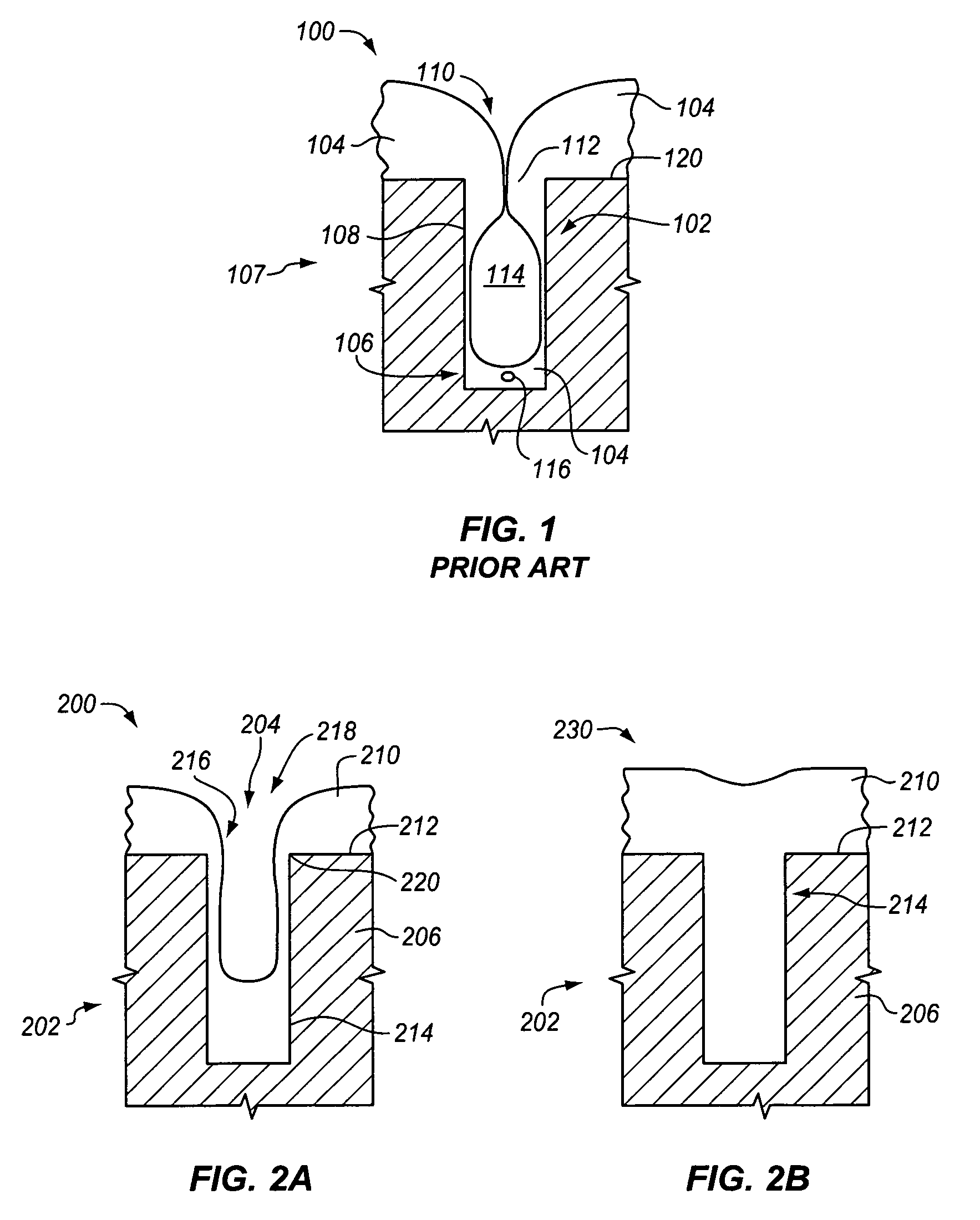
Pulsed bias having high pulse frequency for filling gaps with dielectric material
- Summary
- Abstract
- Description
- Claims
- Application Information
AI Technical Summary
Benefits of technology
Problems solved by technology
Method used
Image

Examples
example 1
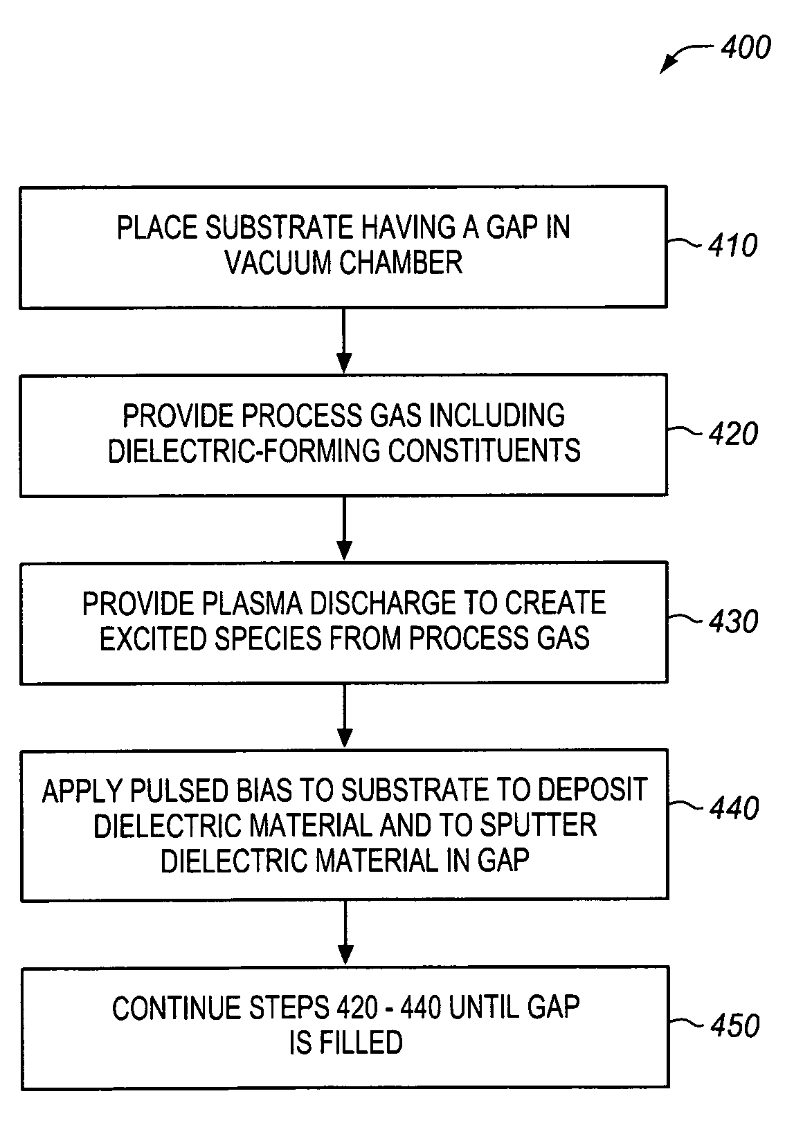
[0075]Using a HDP-CVD process including pulse HF biasing of the substrate in accordance with the invention, partial bottom filling of high AR trenches (gaps) with silicon dioxide (SiO2) dielectric material was conducted with various pulse duty cycle values on a series of semiconductor substrates.
[0076]HDP-CVD deposition processes began by placement of a standard 300 mm semiconductor wafer having high AR trenches on the pedestal of a “SPEED-NexT” HDP-CVD module, commercially available from Novellus Systems, Inc., San Jose, Calif. The trenches had a depth of about 447 nm and a width of 144 nm.
[0077]The process gas compositions and flowrates and HDP-CVD operating conditions were as follows:
[0078]
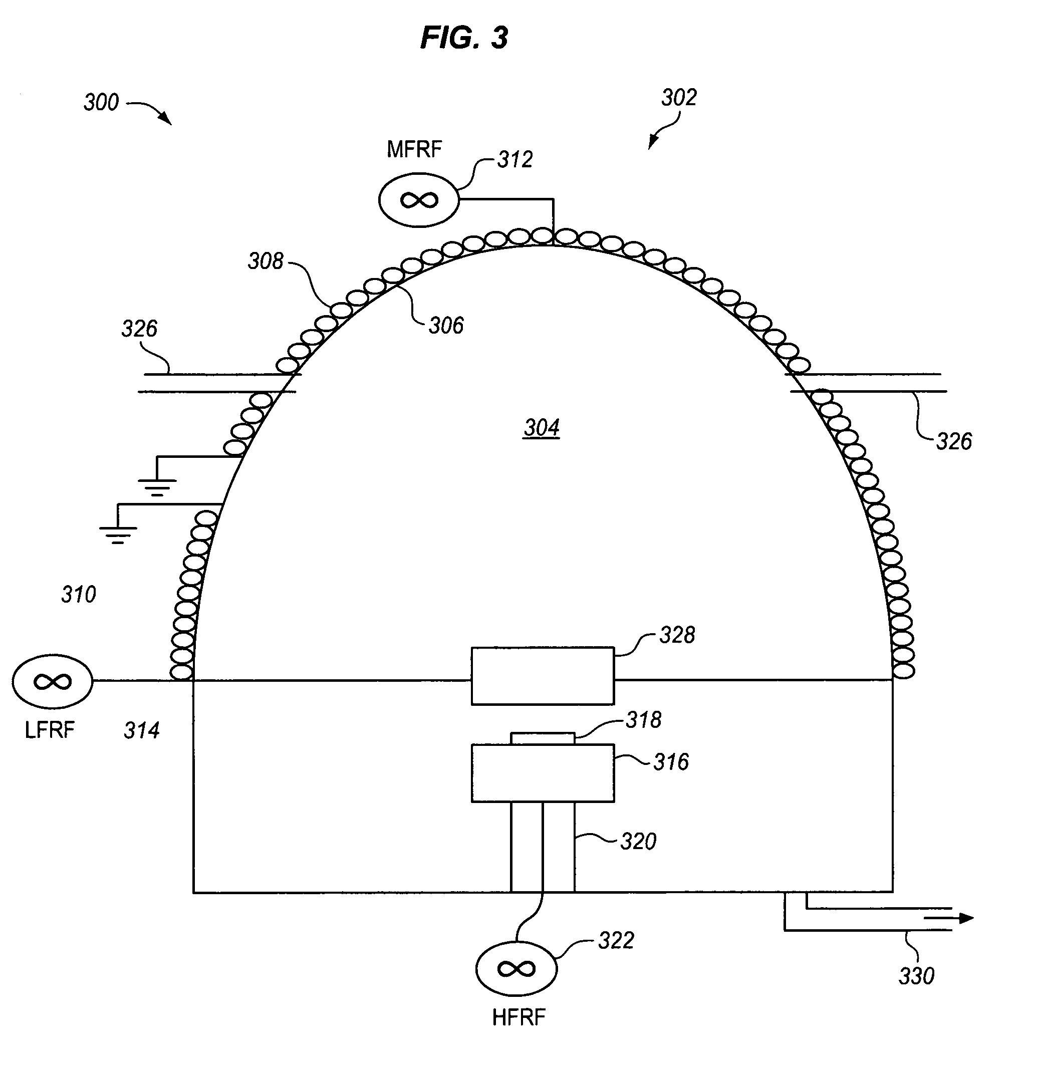
SiH4:50-120 sccmO2:100-600 sccmHe:200-500 sccmH2:250-500 sccmLF-RF:5000 W-8000 WMF-RF:3000 W-5000 WHF-RF:3500 W-5500 WChamber Pressure:approx. 5 mTorrChamber Temperature:approx. 200° C.Substrate Temperature:approx. 550° C.-700° C.Nominal pedestal height:1.5-4Pulse frequency:1 kHz
[0079]HDP-CVD d...
example 2
[0087]Using a HDP-CVD process including pulse HF biasing of the substrate in accordance with the invention, partial bottom filling of high AR trenches (gaps) with silicon dioxide (SiO2) dielectric material was conducted on a series of semiconductor substrates with various combinations of pulse frequency and pulse duty cycle values.
[0088]HDP-CVD deposition processes began by placement of a standard 300 mm semiconductor wafer having high AR trenches on the pedestal of a “SPEED-NexT” HDP-CVD module, commercially available from Novellus Systems, Inc., San Jose, Calif. The trenches had a depth of about 220 nm and a width of 70 nm.
[0089]The process gas compositions and flowrates and HDP-CVD operating conditions were as follows:
[0090]
SiH4:50-120 sccmO2:100-600 sccmHe:200-500 sccmH2:250-500 sccmLF-RF:5000 W-8000 WMF-RF:3000 W-5000 WHF-RF:3500 W-5500 WChamber Pressure:approx. 5 mTorrChamber Temperature:approx. 200° C.Substrate Temperature:approx. 550° C.-700° C.Nominal pedestal height:1.5-4P...
PUM
| Property | Measurement | Unit |
|---|---|---|
| Width | aaaaa | aaaaa |
| Width | aaaaa | aaaaa |
| Depth | aaaaa | aaaaa |
Abstract
Description
Claims
Application Information