Wiring board and method for manufacturing the same

Active Publication Date: 2006-12-21
RENESAS ELECTRONICS CORP
View PDF20 Cites 292 Cited by
  • Summary
  • Abstract
  • Description
  • Claims
  • Application Information

AI Technical Summary

Benefits of technology

[0032] The cross-sectional area based on the via diameter can easily be increased in the present invention by adopting a shape obtained by the partial overlapping of a plurality of similar shapes as the cross-sectional shape of the vias in the plane parallel to the wiring layers. With laser machining in particular, the same shapes can be machined, but forming different shapes only in specific positions is difficult to accomplish. Therefore, specialized machining is dispensed with by creating a shape from partially overlapping similar or identical shapes, and machining can easily be performed with no change in manufacturing cost or output.
[0033] By partially placing the longitudinal axi

Problems solved by technology

Diminished electrical characteristics due to increased wiring resistance have become a problem in this type of multilayer board that uses micro-wiring and an extremely small via diameter.
Specifically, increased wiring resistance creates a situation in which the power source voltage supplied is insufficient for operating the semiconductor e

Method used


Image

  • Wiring board and method for manufacturing the same
  • Wiring board and method for manufacturing the same
  • Wiring board and method for manufacturing the same

Examples


Embodiment Construction

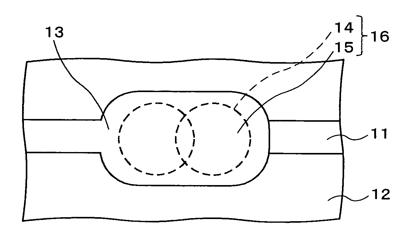
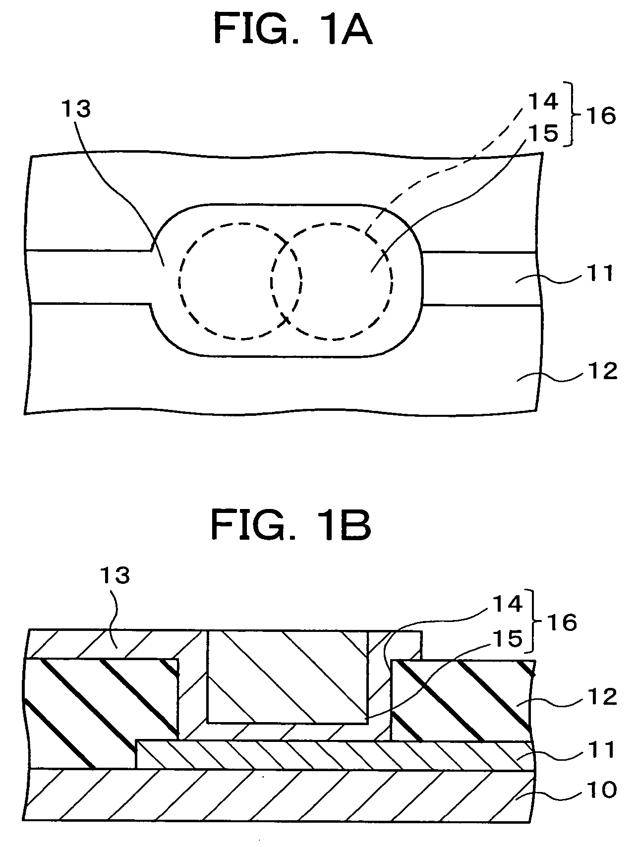
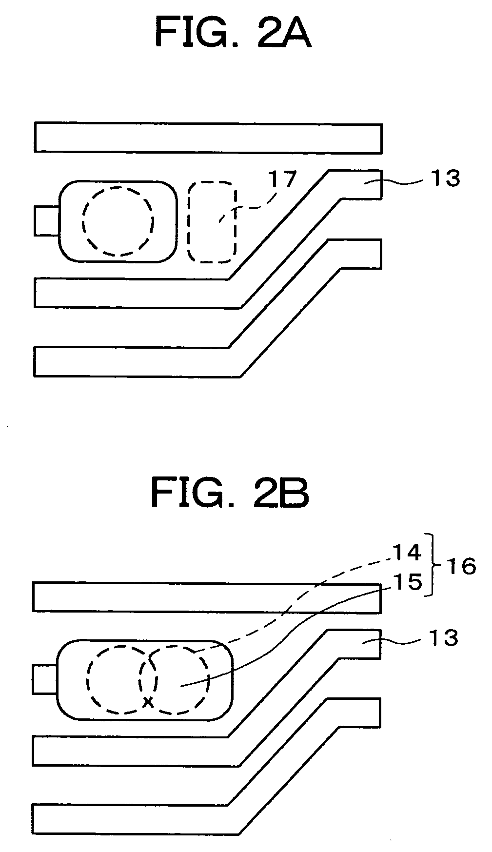
[0042] Embodiments of the present invention will be described in detail hereinafter with reference to the accompanying drawings. The wiring board according to a first embodiment of the present invention will first be described. FIG. 1A is a plan view showing a portion of the wiring board of the present embodiment, and FIG. 1B is a sectional view of the same. In the wiring board shown in FIG. 1, a first wiring layer 11 is provided on a foundation (carrier) board 10, an insulating layer 12 is provided on the first wiring layer 11, and a second wiring layer 13 is furthermore formed on the insulating layer 12. The first wiring layer 11 and the second wiring layer 13 are connected to each other by a via 16 composed of a via hole 14 provided inside the insulating layer 12 and a conductor 15 embedded in the via hole 14.

[0043] The carrier board 10 is composed of a material whereby the surface that is in contact with the bottom face of the first wiring layer 11 has insulating properties. A ...


PUM

PropertyMeasurementUnit
Electrical resistanceaaaaaaaaaa
Densityaaaaaaaaaa
Shapeaaaaaaaaaa

Abstract

A wiring board for mounting a semiconductor element or electronic component having a plurality of wiring layers, an insulating layer provided between these wiring layers, and a via which is provided to the insulating layer and which electrically connects the wiring layers. In this wiring board, the cross-sectional shape of the via in the plane parallel to the wiring layers is obtained by the partial overlapping of a plurality of similar shapes (circles). Stable operation can be obtained in a semiconductor element by minimizing obstacles to increased density, effectively increasing the cross-sectional area of the via, and preventing the wiring resistance from increasing by making the cross-sectional shape of the via into a shape obtained by the partial overlapping of a plurality of similar shapes.

Description

BACKGROUND OF THE INVENTION [0001] 1. Field of the Invention [0002] The present invention relates to a wiring board for mounting a semiconductor element, and to a method for manufacturing the same. The present invention particularly relates to a wiring board in which the connection via structure of the power source and ground is improved, and to a method for manufacturing the same. [0003] 2. Description of the Related Art [0004] Examples of the heretofore used wiring boards for mounting a semiconductor element include ceramic wiring boards such as the one disclosed in Japanese Laid-open Patent Application No. 8-330474 that uses alumina or another insulating material; build-up substrates such as those disclosed in Japanese Laid-open Patent Application No. 11-17058 and Japanese Patent No. 2679681, in which an organic resin is used as the insulating material, and a micro-circuit is formed by forming copper wiring using an etching method and a plating method; and the tape-type substrate...

Claims


Application Information

Patent Timeline
IPC IPC(8): H05K1/11H05K3/42
CPCH05K1/115H05K3/0035H05K3/4069H05K3/421Y10T29/49165H05K2201/09509H05K2201/09854H05K2203/1476H05K3/4644
Inventor KIKUCHI, KATSUMIYAMAMICHI, SHINTAROMURAI, HIDEYAFUNAYA, TAKUOMAEDA, TAKEHIKOHONDA, HIROKAZUOGAWA, KENTATSUKANO, JUN
Owner RENESAS ELECTRONICS CORP
Why Eureka
Try Eureka