Light-emitting diode package

a technology of light-emitting diodes and diodes, which is applied in the direction of semiconductor devices, basic electric elements, electrical equipment, etc., can solve the problems of limited light extraction efficiency and inability to substantially advance, and achieve the effect of improving the extraction efficiency of leds and effective advanced light extraction efficiency

Inactive Publication Date: 2007-11-29
EPISTAR CORP
View PDF6 Cites 45 Cited by
  • Summary
  • Abstract
  • Description
  • Claims
  • Application Information

AI Technical Summary

Benefits of technology

[0009] Accordingly, the present invention is directed to provide a light-emitting diode package (LED package), wherein the LED has better light extraction efficiency.
[0023] In the LED package of the present invention, since both the semiconductor layer and the carrier have a rough surface, the light emitted from the light-emitting layer can be more fully transmitted externally and the light extraction efficiency of the LED is effectively advanced. In addition, the present invention further provides a LED package, wherein the semiconductor layer has a rough surface and the carrier has a reflective layer, such that extraction efficiency of the LED can be improved.

Problems solved by technology

However, as the light emitted from the light-emitting layer is reflected by the reflective layer and then the most light travels through the semiconductor layer, the light could be absorbed by the semiconductor layer; therefore the light extraction efficiency of the LED is limited and can not be substantially advanced.

Method used


Image

  • Light-emitting diode package
  • Light-emitting diode package
  • Light-emitting diode package

Examples


Embodiment Construction

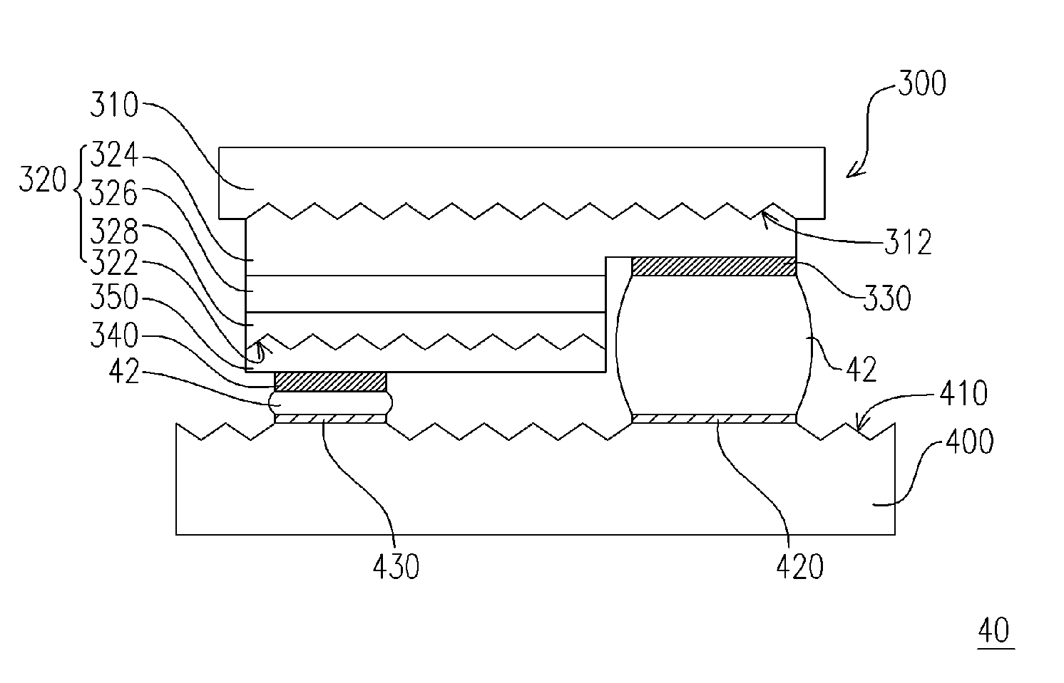
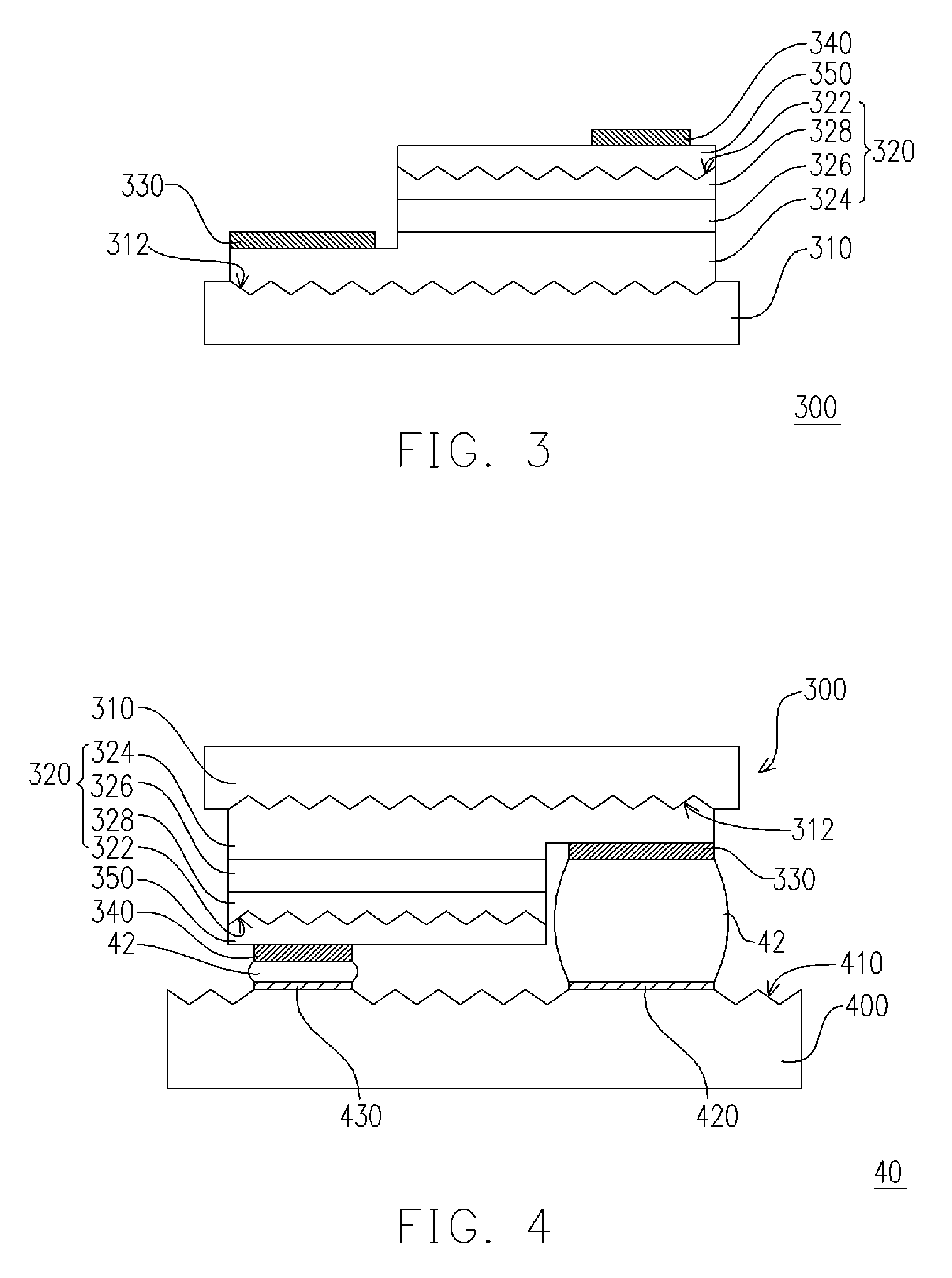
[0030] The LED package of the present invention includes a LED and a carrier, wherein the LED is electrically coupled to the carrier through flip-chip interconnecting technology. In the embodiment, the LED can be a white LED chip, an ultraviolet LED chip or other LEDs suitable for emitting different color lights. The carrier can be a substrate or a lead frame. In the following, a LED package of an embodiment in the present invention is described in detail.

[0031]FIG. 3 is a LED diagram of a LED package according to an embodiment of the present invention. Referring to FIG. 3, the LED 300 of the present invention mainly includes a substrate 310, a semiconductor layer 320, a first electrode 330 and a second electrode 340. In the present embodiment, the semiconductor layer 320 is disposed on the substrate 310 and has a rough surface 322. In addition, the semiconductor layer 320 includes a first-type doped semiconductor layer 324, a light-emitting layer 326 and a second-type doped semico...


PUM


Abstract

A light-emitting diode package (LED package) includes a LED and a carrier. The LED includes a substrate, a semiconductor layer, a first electrode and a second electrode. The semiconductor layer is located on a surface of the substrate and has a rough surface. The semiconductor layer includes a first-type doped semiconductor layer, a second-type doped semiconductor layer and a light-emitting layer disposed between the two doped semiconductor layers. The first electrode and the second electrode are disposed on and electrically coupled the first-type doped semiconductor layer and the second-type doped semiconductor layer, respectively. The carrier has a rough carrying surface and includes a first contact pad and a second contact pad disposed on the rough carrying surface. The first electrode and the second electrode of the LED face the carrier and are electrically coupled to the first contact pad and a second contact pad, respectively.

Description

BACKGROUND OF THE INVENTION [0001] 1. Field of Invention [0002] The present invention relates to a semiconductor device structure, and particularly to a light-emitting diode package (LED package). [0003] 2. Description of the Related Art [0004] The light-emitting diode (LED) formed by semiconductor material of the compound of the group III-V elements is a wide bandgap luminous component, which emits the light covering all wavebands of visible light. In recent years, following the progress towards high-chroma and extreme-brightness, LEDs have gained broader applications fields, such as mega-size outdoor display boards and traffic lights, and would even substitute tungsten lamps and mercury lights to become a future lighting source with energy-saving and environmentally friendly advantages. [0005] The LED basic structure includes a semiconductor layer. The semiconductor layer comprises a P-type doped semiconductor layer, an N-type doped semiconductor layer and a light-emitting layer d...

Claims


Application Information

Patent Timeline
Patent Type & Authority Applications(United States)
IPC IPC(8): H01L33/00H01L33/22H01L33/60
CPCH01L33/60H01L33/22H01L2224/16225
Inventor TSENG, HUAN-CHEWEN, WAY-JZEPAN, SHYI-MING
Owner EPISTAR CORP
Why Eureka
Try Eureka