High power light emitting diode package and method of producing the same

a light-emitting diode and high-power technology, applied in the direction of electrical equipment, semiconductor/solid-state device manufacturing, semiconductor devices, etc., to achieve the effect of increasing the efficiency of light extraction and high-power led

Active Publication Date: 2008-02-21
SAMSUNG ELECTRONICS CO LTD
View PDF10 Cites 65 Cited by
  • Summary
  • Abstract
  • Description
  • Claims
  • Application Information

AI Technical Summary

Benefits of technology

[0010]The present invention has been made to solve the foregoing problems of the prior art and therefore an aspect of the present invention is to provide a high power LED package which prevents interference of light beams among adjacent LED chips, thereby effectively increasing the light extraction efficiency, and a method of producing the same.

Problems solved by technology

In addition, the package body may expose a portion of undersurface of the base of the first lead frame.

Method used


Image

  • High power light emitting diode package and method of producing the same
  • High power light emitting diode package and method of producing the same
  • High power light emitting diode package and method of producing the same

Examples


Embodiment Construction

[0024]Exemplary embodiments of the present invention will now be described in detail with reference to the accompanying drawings. The invention may however be embodied in many different forms and should not be construed as limited to the embodiments set forth herein. Rather, these embodiments are provided so that this disclosure will be thorough and complete, and will fully convey the scope of the invention to those skilled in the art. In the drawings, the shapes and dimensions may be exaggerated for clarity and the same reference numerals are used throughout to designate the same or like components.

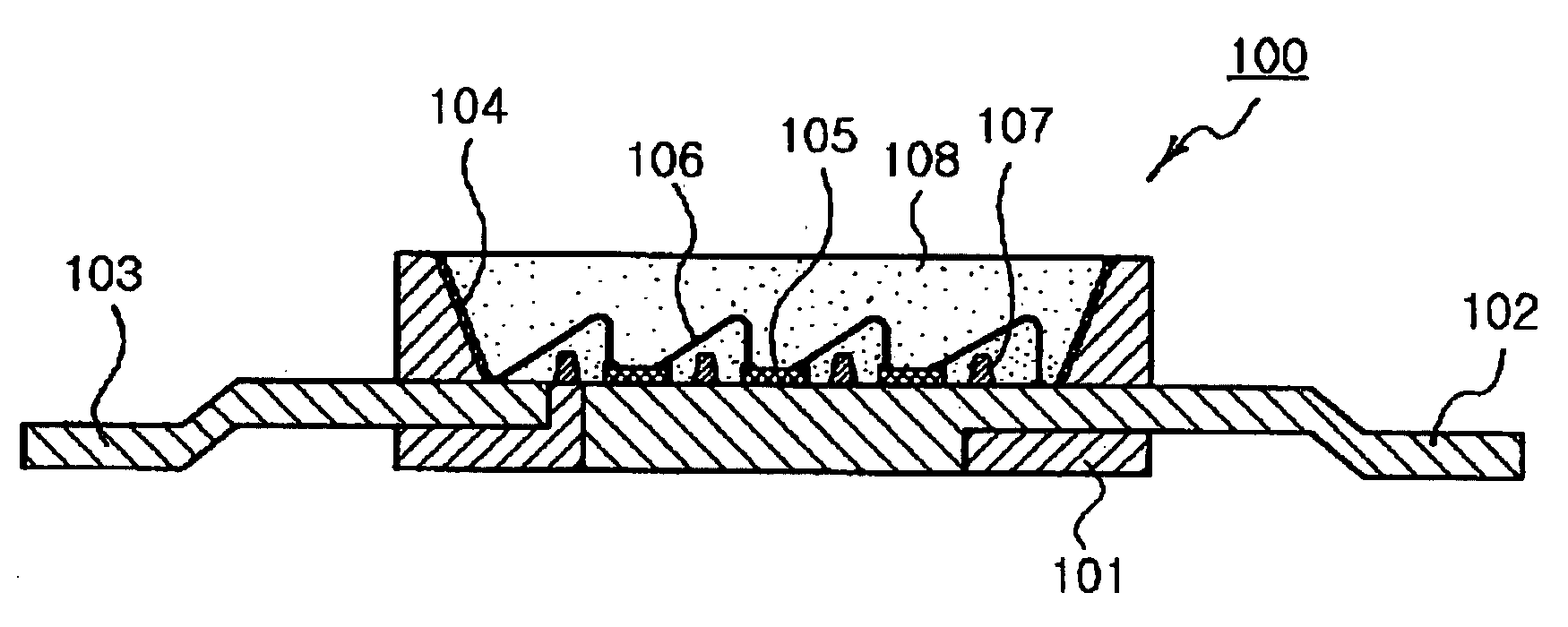
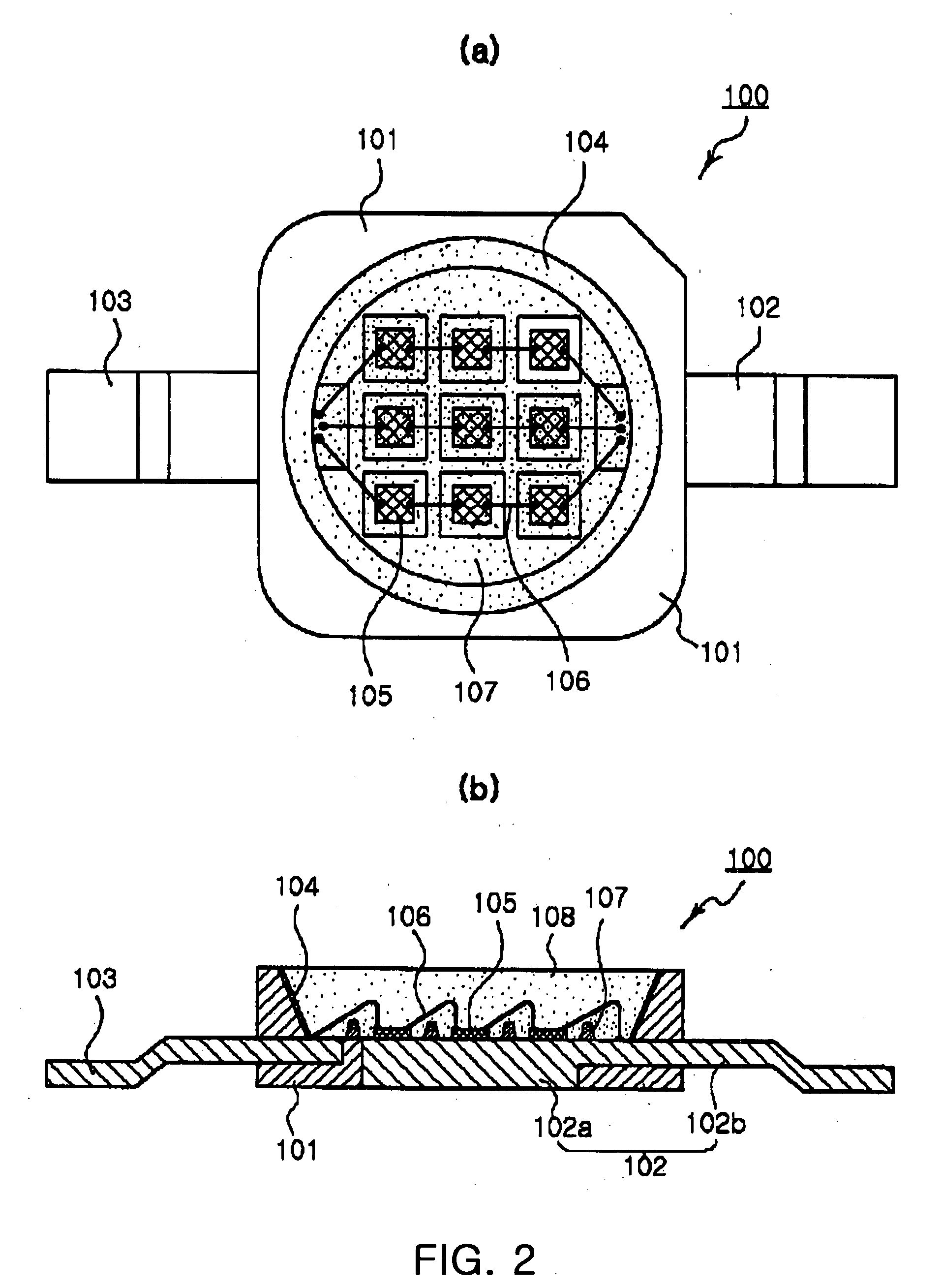
[0025]FIG. 2(a) and (b) are a plan view and a sectional view illustrating a high power LED package 100 according to the present invention.

[0026]Referring to FIGS. 2(a) and (b), the high power LED package 100 according to the present invention includes a plurality of LED chips 105, a first lead frame 102, a second lead frame 103, a package body 101 having at least one first reflecting par...


PUM


Abstract

A high power Light Emitting Diode (LED) package and a method of producing the same. The high power LED package according to the present invention includes a plurality of light emitting diode chips, a first lead frame with the light emitting diode chips mounted thereon, and a second lead frame disposed at a predetermined interval from the first lead frame. The LED package also includes a package body fixing the first and second lead frames and bonding wires for electrically connecting the plurality of LED chips. The package body includes at least one first reflecting part separately surrounding each of the plurality of LED chips with upward-inclined inner side walls thereof and a second reflecting part surrounding the entire plurality of LED chips with an upward-inclined inner side wall thereof.

Description

CLAIM OF PRIORITY[0001]This application claims the benefit of Korean Patent Application No. 2006-0064439 filed on Jul. 10, 2006, in the Korean Intellectual Property Office, the disclosure of which is incorporated herein by reference.BACKGROUND OF THE INVENTION[0002]1. Field of the Invention[0003]The present invention relates to a high power Light Emitting Diode (LED) package and a method of producing the same and, more particularly, to a high power LED package which can effectively increase the light extraction efficiency, and a method of producing the same.[0004]2. Description of the Related Art[0005]In general, LEDs, which convert electric signals to light using characteristics of compound semiconductors, have advantages such as longer lifetime than other types of light emitters, low driving voltage and low power consumption. In addition, LEDs have a high response rate, high resistance to impacts, and readily accommodate miniaturization and light-weight applications.[0006]With the...

Claims


Application Information

Patent Timeline
Patent Type & Authority Applications(United States)
IPC IPC(8): H01L33/00H01L33/46H01L33/48H01L33/60
CPCH01L25/0753H01L33/46H01L2924/3025H01L2224/49113H01L2224/48471H01L2224/48465H01L2924/01322H01L2224/48247H01L2224/48137H01L2224/48091H01L33/60H01L33/486H01L2924/00014H01L2924/00
Inventor OH, KYUNG SEOBROH, JAE KYPARK, JUNG KYUBAEK, JONG HWANCHOI, SEUNG HWAN
Owner SAMSUNG ELECTRONICS CO LTD
Why Eureka
Try Eureka