
Silicone adhesive for semiconductor element

a silicon adhesive and semiconductor technology, applied in the direction of non-macromolecular adhesive additives, transportation and packaging, layered products, etc., can solve the problems of deterioration in light extraction efficiency, deterioration in light reflection efficiency, and reduction in brightness, so as to achieve effective reflection of light emitted, improve light extraction efficiency, and high degree of concealment

Inactive Publication Date: 2009-10-15
SHIN ETSU CHEM IND CO LTD
View PDF3 Cites 49 Cited by
  • Summary
  • Abstract
  • Description
  • Claims
  • Application Information

AI Technical Summary

Benefits of technology

[0008]The present invention has been developed in light of the above circumstances, and has an object of providing a silicone adhesive for a semiconductor element that exhibits a high degree of concealment, effectively reflects light emitted from LED chips, and can be used as a die bonding material.
[0019]The present invention is able to provide a silicone adhesive for a semiconductor element that exhibits a high degree of concealment and effectively reflects light emitted from LED chips, thereby improving the light extraction efficiency. This adhesive also produces favorable chip positioning properties, and exhibits a high level of adhesive strength and excellent durability. Incidentally, herein, what is meant by the adhesive having favorable chip positioning properties, is that when a tip is placed and pressed on the adhesive applied on a substrate, the chip can be placed well at a desired position without deviation, lift or the like.DETAILED

Problems solved by technology

However, die bonding materials used for fixing blue or white LED light emitting elements (chips) tend to yellow over time upon extended use, and in a similar manner to that observed for epoxy encapsulating materials, the die bonding material tends to absorb light, causing a reduction in the brightness.
Silver electrodes and gold electrodes are typically used for LED electrodes, but in those cases where a silver electrode is used, oxygen permeation or the like through the encapsulating material can cause oxidation and blackening of the surface of the silver electrode, resulting in a deterioration in the light reflection efficiency.
However, if a transparent silicone die bonding material such as that disclosed in Patent Document 1 is used with a gold electrode, then a problem arises in that the light emitted from the LED chip is absorbed at the gold surface, causing a deterioration in the light extraction efficiency.

Method used


Image

  • Silicone adhesive for semiconductor element
  • Silicone adhesive for semiconductor element
  • Silicone adhesive for semiconductor element

Examples


example 1

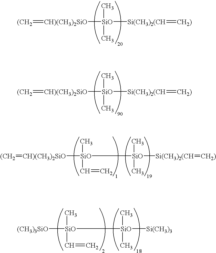
[0070](1) A linear dimethylpolysiloxane (A1) with both terminals blocked with vinyl groups and having a viscosity at 25° C. of 70 mPa·s,

[0071]a toluene solution of a silicone resin (B1) composed of Me3SiO1 / 2, ViMe2SiO1 / 2 (wherein Vi represents a vinyl group, this definition also applies below) and SiO4 / 2 units, with a molar ratio of the combination of the Me3SiO1 / 2 and ViMe2SiO1 / 2 units relative to the SiO4 / 2 units of 0.8, and having an amount of vinyl groups relative to the solid fraction of 0.085 mols / 100 g, and

[0072]a methylhydrogensiloxane (C1) of the above average composition formula (2): R4aHbSiO(4−a−b) / 2 wherein R4 represents a methyl group, a=1.44 and b=0.78, with both terminals blocked with trimethylsiloxy groups, and having a viscosity at 25° C. of 7.5 mPa·s

[0073]were mixed together in a solid fraction equivalent mass ratio of 25:75:10. The toluene was removed from the resulting mixture by treatment at 120° C. under a reduced pressure of not more than 10 mmHg, thereby yiel...

example 2

[0075]The silicone base 1 was prepared in the same manner as example 1, and to 100 parts by mass of this silicone base 1 were added 50 parts by mass of the same titanium oxide powder (b1) used in example 1, 90 parts by mass of an alumina powder (c2) having an average particle size of 4.0 μm (product name: AL-43PC, manufactured by Showa Denko K.K.), and the same platinum catalyst (D1) used in example 1, in sufficient amount to provide the equivalent of 10 ppm of platinum atoms relative to the silicone component. The mixture was then stirred thoroughly, and 3 parts by mass of a hydrocarbon solvent with a boiling point of at least 200° C. was added, yielding a white paste with a viscosity of 20 Pa·s.

example 3

[0076]A mixture containing 45.8 g of vinylmethyldichlorosilane, 111.0 g of phenyltrichlorosilane (molar ratio 38:62) (average composition of mixture: (CH3)0.38(C6H5)0.62(CH2═CH)0.38SiO1.31) and 20 g of toluene was added gradually, in a dropwise manner, to a mixture of 120 g of toluene and 320 g of water being stirred inside a flask, with the addition controlled so that the temperature inside the flask did not exceed 50° C., thereby effecting a cohydrolysis. A polycondensation was then conducted by continuing the reaction at not more than 70° C. for two hours, thus forming a toluene solution of a three dimensional network structure organopolysiloxane (silicone resin) (P1) that exhibited a non-volatile component of 70% when heated for 30 minutes at 150° C. The solid fraction (P1) within this solution existed in a non-fluid gum-like state at 25° C. This organopolysiloxane solution was stripped for one hour under conditions of 80° C. and 15 mmHg, and to 100 parts by mass of the resultin...


PUM

PropertyMeasurementUnit
viscosityaaaaaaaaaa
particle sizeaaaaaaaaaa

Abstract

A silicone adhesive for a semiconductor element that is suitable as a die bonding material for fixing a light emitting diode chip to a substrate. The adhesive includes (a) an addition reaction-curable silicone resin composition having a viscosity at 25° C. of not more than 100 Pa·s, and yielding a cured product upon heating at 150° C. for 3 hours that has a type D hardness prescribed in JIS K6253 of at least 30, (b) a white pigment powder having an average particle size of less than 1 μm, and (c) a white or colorless and transparent powder having an average particle size of at least 1 μm but less than 10 μm. The adhesive exhibits high levels of concealment, effectively reflects light emitted from the LED chip, and also exhibits favorable chip positioning properties, superior adhesive strength, and excellent durability.

Description

BACKGROUND OF THE INVENTION[0001]1. Field of the Invention[0002]The present invention relates to a white die bonding material that is suitable for fixing a light emitting diode (LED) chip to a gold-plated substrate. More specifically, the invention relates to a heat-curable silicone adhesive for a semiconductor element that produces favorable chip positioning properties when a chip is pressed onto a substrate, exhibits high levels of concealment and adhesive strength, displays excellent durability, and effectively reflects light emitted from the chip.[0003]2. Description of the Prior Art[0004]Epoxy resins have conventionally been used as the die bonding material for fixing LED light emitting elements (chips). However, die bonding materials used for fixing blue or white LED light emitting elements (chips) tend to yellow over time upon extended use, and in a similar manner to that observed for epoxy encapsulating materials, the die bonding material tends to absorb light, causing a red...

Claims


Application Information

Patent Timeline
Patent Type & Authority Applications(United States)
IPC IPC(8): B32B7/12C09J183/00C09J183/06C09J11/04C09J183/04C09J183/05C09J183/07H01L21/52H01L33/48H01L33/50
CPCY10T428/25H01L33/56C09J183/14
Inventor YAMAKAWA, NAOKIMIYOSHI, KEIOZAI, TOSHIYUKIOGAWA, YOSHINORI
Owner SHIN ETSU CHEM IND CO LTD
Learn More