Light emitting diode package and method of manufacturing the same

a technology of light-emitting diodes and led packages, which is applied in the direction of semiconductor/solid-state device manufacturing, semiconductor devices, electrical equipment, etc., can solve the problems of not being suitable for lighting devices, cameras, mobile phones, etc., and achieves the effects of improving the structure, easy manufacturing, and enhancing the light extraction rate of led packages

Active Publication Date: 2008-06-19
SAMSUNG ELECTRONICS CO LTD
View PDF8 Cites 59 Cited by
  • Summary
  • Abstract
  • Description
  • Claims
  • Application Information

AI Technical Summary

Benefits of technology

[0018]An advantage of the present invention is that it provides an LED package of which the structure is improved so that the LED package can be easily manufactured. Further, a light extraction rate of the LED package is enhanced so that light extraction efficiency can be enhanced, while the LED package can be reduced in thickness.
[0019]Another advantage of the invention is that it provides a method of manufacturing an LED package.
[0020]Additional aspect and advantages of the present general inventive concept will be set forth in part in the description which follows and, in part, will be obvious from the description, or may be learned by practice of the general inventive concept.
[0021]According to an aspect of the invention, an LED package comprises a frame having a concave portion formed in the center thereof; one or more LED chips mounted on the bottom surface of the concave portion; and a lens filled in the concave portion, the lens having an upper surface formed of continuous prismatic irregularities forming concentric circles.
[0022]Preferably, the side of the concave portion is formed in a tapered shape expanding upward.
[0023]Preferably, the frame has an upper opening formed in a circular shape, and the lower circumference of the lens is formed in a shape corresponding to the shape of the upper opening of the frame.

Problems solved by technology

Therefore, such LED packages are not suitable for lighting devices, cameras, or mobile phones which require an ultra-slim structure.
However, the height of the LED package inevitably increases as much as the diameter of the hemispheric lens, which means that the package having a hemispheric lens is not suitable for flashes of mobiles phones and the like.

Method used


Image

  • Light emitting diode package and method of manufacturing the same
  • Light emitting diode package and method of manufacturing the same
  • Light emitting diode package and method of manufacturing the same

Examples


first embodiment

of LED Package

[0078]Referring to FIGS. 5 and 6, an LED package according to a first embodiment of the invention will be described.

[0079]FIG. 5 is a perspective view of an LED package according to a first embodiment of the invention, and FIG. 6 is a cross-sectional view of FIG. 5.

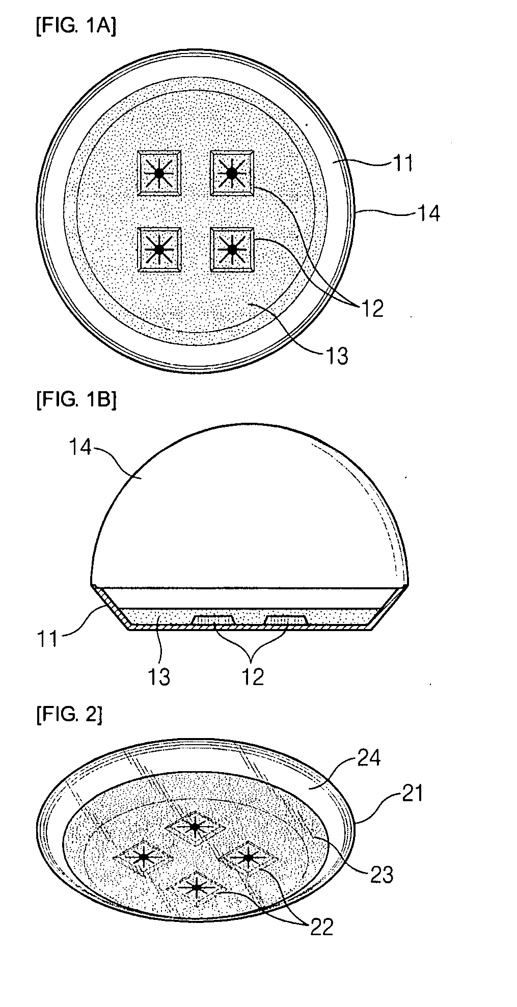
[0080]As shown in FIGS. 5 and 6, the LED package according to the first embodiment of the invention includes a frame 111 having a concave portion formed in the center thereof, one or more LED chips 112 mounted on the bottom surface of the concave portion, and a lens 114 filled in the concave portion and having an upper surface formed of continuous prismatic irregularities 114 forming concentric circles.

[0081]Preferably, the side of the concave portion is formed in a tapered shape expanding upward.

[0082]The side shape of the concave portion and the inclined angle of the tapered shape are properly set in accordance with the specification of an LED package. However, like a flash light source of a camera, it is ...

second embodiment

of LED Package

[0096]Referring to FIGS. 9 and 10, an LED package according to a second embodiment of the invention will be described.

[0097]As shown in FIGS. 9 and 10, the LED package according to the second embodiment of the invention includes a frame 211 having a concave portion formed in the center thereof, one or more LED chips 212 mounted on the bottom surface of the concave portion, and a lens 214 filled in the concave portion, the lens 214 having an upper surface formed of a Fresnel lens surface 214a.

[0098]That is, the LED package according to the second embodiment of the invention has a Fresnel lens surface 214a formed thereon, instead of the continuous prismatic irregularities 114a forming concentric circles.

[0099]The Fresnel lens surface 214a can serve as a convex lens while the thickness thereof is reduced. Therefore, although the lens 214 has a small thickness like an existing flat lens, the lens 214 has a much more excellent light extraction rate than the flat lens.

[0100...

third embodiment

of LED Package

[0114]Referring to FIGS. 12 and 13, an LED package according to a third embodiment of the invention will be described.

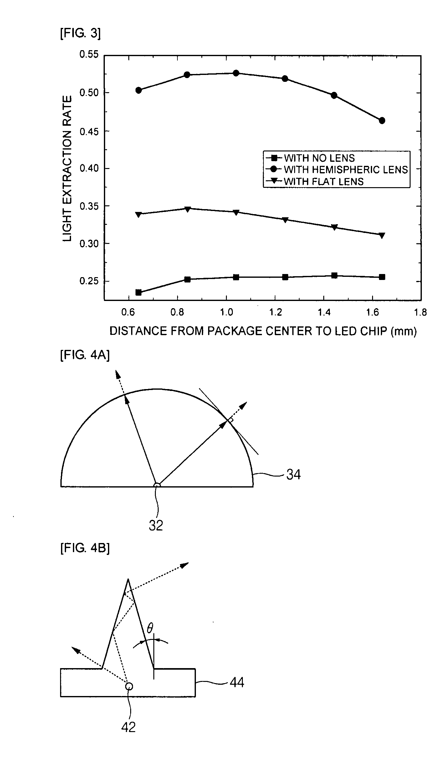
[0115]As shown in FIGS. 12 and 13, the LED package according to the third embodiment of the invention includes a frame 311 having a concave portion in the center thereof, one or more LED chips 312 mounted on the bottom surface of the concave portion, and a flat dome lens 314 filled in the concave portion.

[0116]That is, the LED package according to the third embodiment of the invention has a flat dome lens according to the angle division technique which is newly tried in the invention.

[0117]More specifically, the flat dome lens 314 is formed as follows. Referring to FIG. 4D, a hemispheric lens is divided into a suitable number of predetermined angles θ from a line connecting one end of the reflecting frame 311 and the center of the hemispheric lens 316 where it is assumed that a point light source O is located in the center of the lens. In FIG. 4D, the n...


PUM


Abstract

An LED package comprises a frame having a concave portion formed in the center thereof; one or more LED chips mounted on the bottom surface of the concave portion; and a lens filled in the concave portion, the lens having an upper surface formed of continuous prismatic irregularities forming concentric circles.

Description

CROSS-REFERENCE TO RELATED APPLICATIONS[0001]This application claims the benefit of Korean Patent Application No. 10-2006-0127324 filed with the Korea Intellectual Property Office on Dec. 13, 2006, the disclosure of which is incorporated herein by reference.BACKGROUND OF THE INVENTION[0002]1. Field of the Invention[0003]The present invention relates to a light emitting diode (LED) package, which can be easily manufactured and has an enhanced light extraction rate such that light extraction efficiency can be enhanced, while being reduced in thickness, and a method of manufacturing the same.[0004]2. Description of the Related Art[0005]In general, LEDs generate minority carriers (electrons and holes) injected by using a p-n junction structure of semiconductor and then recombine them to emit light. That is, when a forward voltage is applied to a semiconductor of a specific element, electrons and holes are recombined through migration in a positive-negative junction. Then, energy level i...

Claims


Application Information

Patent Timeline
Patent Type & Authority Applications(United States)
IPC IPC(8): H01L33/00H01L33/22H01L33/54H01L33/56H01L33/60
CPCH01L33/54H01L25/0753H01L2924/0002H01L2924/1815H01L2924/00
Inventor KIM, HYUN JUNCHOI, CHANG HWANLEE, JONG MYEONKIM, DONG WOOHNMOON, WON HA
Owner SAMSUNG ELECTRONICS CO LTD
Why Eureka
Try Eureka