Memory including a performance test circuit

a performance test circuit and memory technology, applied in the field of memory, can solve the problems of increasing the size (in terms of silicon surface area) of the integrated circuit memory, increasing the complexity of the manufacturing method, and variability in the performance of the integrated circuit, so as to facilitate the making of the test cell and limit the overall memory consumption

Active Publication Date: 2009-06-18
STMICROELECTRONICS SRL
View PDF21 Cites 378 Cited by
  • Summary
  • Abstract
  • Description
  • Claims
  • Application Information

AI Technical Summary

Benefits of technology

[0017]A test cell is thus made almost identically to a memory cell, the sole difference between the two then being the absence of a link between the output of the second inverter and the input of the first inverter. The making of the test cells is thus facilitated and their performance is as close as possible to that of the memory cells.
[0018]In one variant, the test circuit (200) may also include an inhibition circuit to open the looped chain when it receives a test control signal (VAL). The inhibition circuit thus enables the deactivation of the looped chain (i.e. the test circuit) outside the phases in which the memory is tested, thus limiting overall memory consumption.

Problems solved by technology

The complexity of integrated circuits (the growing number of memory elements, the ever smaller surface area of each memory cell, etc.) goes together with a corresponding increase in the complexity of the manufacturing methods and the variability in the performance of integrated circuits, related to the manufacturing method, i.e. the variability in the performance of the integrated memories coming from a same silicon wafer or from a same batch of wafers.
It significantly increases the size (in terms of silicon surface area) of the integrated circuit memory and lowers its performance.

Method used


Image

  • Memory including a performance test circuit
  • Memory including a performance test circuit

Examples


Embodiment Construction

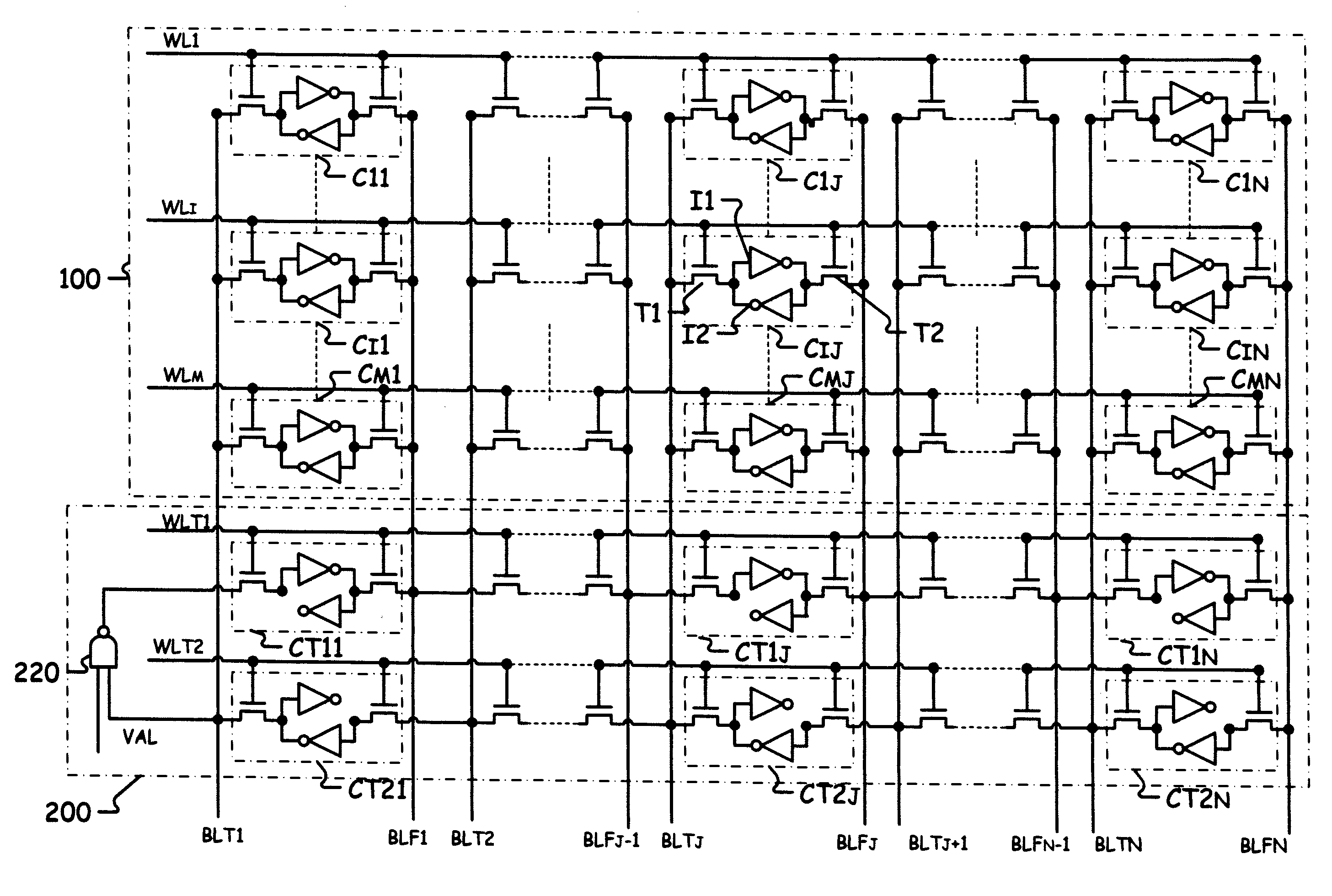
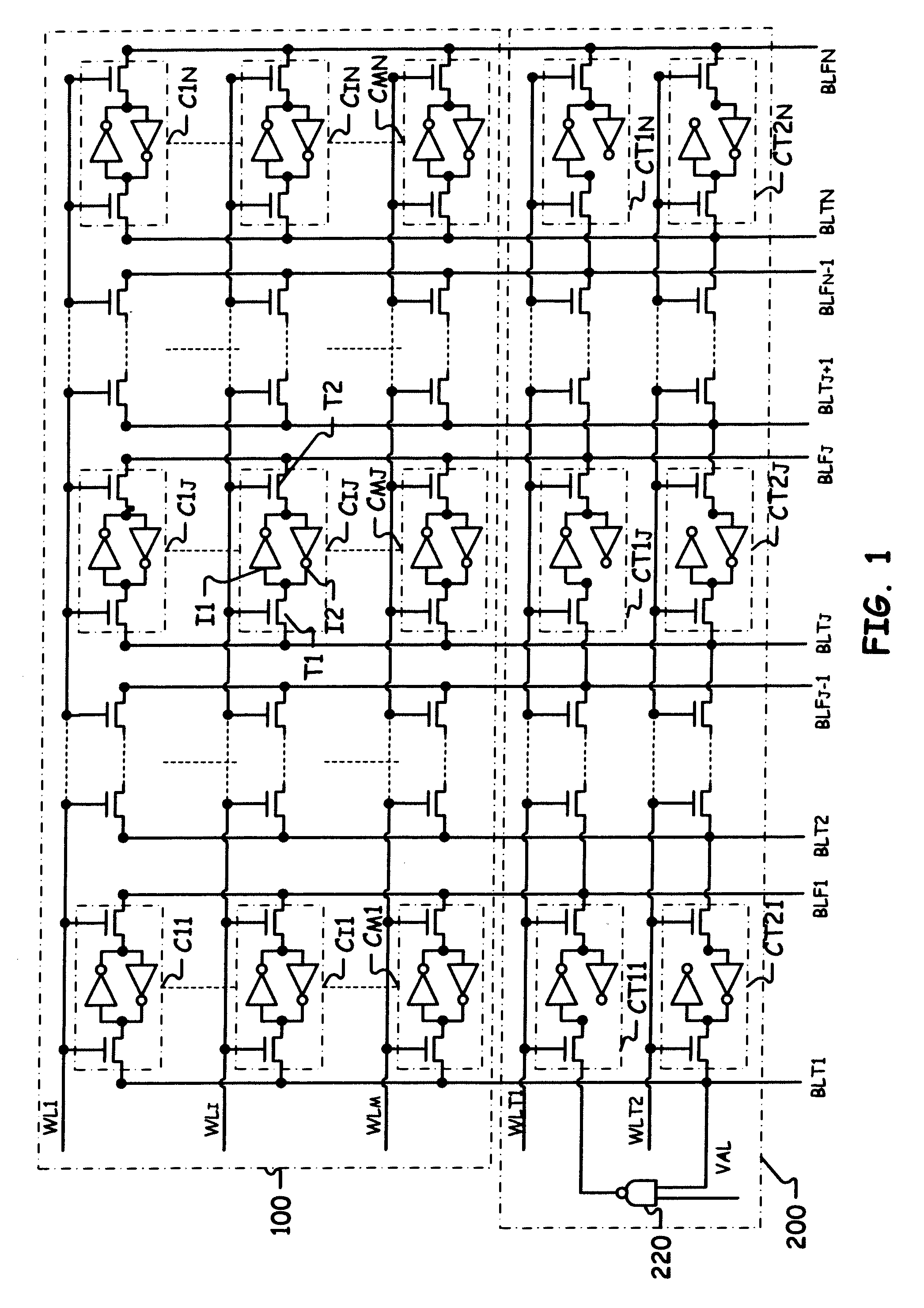
[0022]As stated here above, a memory according to the invention, like a prior-art memory, comprises a memory area 100 comprising a plurality of memory cells C11, . . . C1N, C21, . . . , CM1, CMN, distributed among M memory words WORD1, . . . , WORDM each comprising N memory cells C11 to C1N, C21 to C2N, . . . , CM1 to CMN, where M and N are integers and M*N is the size (in terms of storage capacity) of the memory.

[0023]All the cells of a same word WORDi (cells C11 to C1N of the word WORD1, cells C21 to C2N of the word WORD2, . . . , cells CM1 to CMN of the word WORDN) also have a control input connected to a same word line WLi ranked (WL1, WL2, . . . or WLN), and all the cells of a same rank j from 1 to N of each of the words WORD1, WORD2, WORDN each have a true data input connected to a bit line BLTj ranked j and a complementary data input linked to a complementary bit line BLFj ranked j.

[0024]Each cell Cij has a memory element comprising two inverters I1, I2 connected head-to-tail...


PUM


Abstract

A memory includes a plurality of memory cells each including a true data input connected to a true bit line and complementary data input connected to a complementary bit line, and two inverters connected head-to-tail firstly to the true data input and secondly to the complementary data input. The memory also includes a test circuit includes a plurality of test cells, each test cell includes a true data input connected to a complementary data input of the preceding test cell and a complementary data input connected to the true data input of the following test cell, the complementary data input of the last test cell being connected to the true data input of the first test cell, each test cell comprising a first inverter connected between the true data input and the complementary data input. The looped chain thus formed propagates a signal whose period is a function of the performance of the storage cells.

Description

RELATED APPLICATION[0001]The present application claims priority of French Patent Application No. 0759905 filed Dec. 17, 2007, which is incorporated herein in its entirety by this reference.FIELD OF THE INVENTION[0002]The invention pertains to a memory comprising a plurality of memory cells each comprising a true data input connected to a true bit line and a complementary data input connected to a complementary bit line, and two inverters connected head-to-tail firstly to the true data input and secondly to the complementary data input.RELEVANT BACKGROUND[0003]The plurality of memory cells is most commonly distributed over a memory area comprising M memory words each comprising N memory cells where M and N are integers and M*N is the size of the memory. Each of the memory cells of a same word also has a control input connected to a same word line and each of the same-ranking cells of each of the words has a data input connected to a same-ranking bit line and a complementary data inp...

Claims


Application Information

Patent Timeline
Patent Type & Authority Applications(United States)
IPC IPC(8): G11C29/00G11C7/00
CPCG11C11/41G11C29/50012G11C29/50G11C29/24
Inventor BOROT, BERTRANDBECHET, EMMANUEL
Owner STMICROELECTRONICS SRL
Why Eureka
Try Eureka