Carbon nanotube structures, carbon nanotube devices using the same and method for manufacturing carbon nanotube structures

a carbon nanotube and carbon nanotube technology, applied in the direction of instruments, semiconductor/solid-state device details, transportation and packaging, etc., can solve the problems of difficult handling, difficult handling and expensiveness, and the production of a single type of carbon nanotubes has not yet been achieved, so as to achieve less carbon nanotube structures and easy manufacturing

Inactive Publication Date: 2005-07-26
FUJIFILM BUSINESS INNOVATION CORP
View PDF2 Cites 385 Cited by
  • Summary
  • Abstract
  • Description
  • Claims
  • Application Information

AI Technical Summary

Benefits of technology

[0037]The invention is designed to provide carbon nanotube structures, in which networks with a desired area and volume, where carbon nanotubes are electrically or magnetically connected, are formed and the method for easy manufacturing the carbon nanotube structures with less carbon nanotube structures. The invention is also designed to provide carbon nanotube devices, to which such useful carbon nanotube structures mentioned above are applied.

Problems solved by technology

Type of carbon nanotubes may be determined depending on how to synthesize and the established conditions to some degree but production of purely one type of the carbon nanotubes has not yet been achieved.
For example, since when an attempt was made to apply the carbon nanotubes to electric circuits, not only was it difficult to handle the carbon nanotubes because of their very fine sizes but also no method had been yet proposed for producing high-density wiring such as integrated circuits (ICs), the only thing subject to evaluation was that a single-structure fine element, which was produced by preparing fine electrodes, on which the carbon nanotubes were grown as shown in “Nature” (vol.
The problems of difficult handling and expensiveness are large obstacles to actual application to devices.
Nevertheless, it has not yet been reported that a structure of carbon nanotubes and fibers was used to transmit and process signals.
In the case of using conductive particles as fine objects, if they can be distributed into a network, even a small amount of fine objects allow the whole surface of the board to be conductive, although, as mentioned above, only by drying the dispersion medium from the liquid with the fine objects dispersed, the domain is prone to being stably formed of plural separate islands of the fine objects.
This has been an obstacle to forming a useful network for a carbon nanotube structure.
In this case, since a remarkably large amount of carbon nanotubes are required, there is no merit found in the use of carbon nanotubes.

Method used


Image

  • Carbon nanotube structures, carbon nanotube devices using the same and method for manufacturing carbon nanotube structures
  • Carbon nanotube structures, carbon nanotube devices using the same and method for manufacturing carbon nanotube structures
  • Carbon nanotube structures, carbon nanotube devices using the same and method for manufacturing carbon nanotube structures

Examples


first embodiment

(First Embodiment)

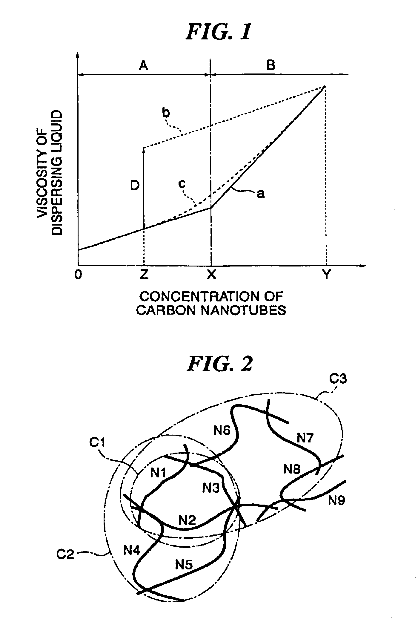
[0162]FIG. 8 is a schematic perspective view showing a first embodiment of the carbon nanotube structure of the invention. A carbon nanotube structure 68 made of the carbon nanotubes 64 is fixed on almost the whole surface of a planar board 62. The carbon nanotubes 64 with several μm to several-ten μm in length are in contact with each other to form an electric conductive network. For this reason, conductivity is attained on the surface of the planar board 62. FIG. 9 is an electronic microscopic picture (magnified by a factor of 30000) showing the carbon nanotube structures 68, which is an embodiment of the invention. Note that some error has occurred in the magnification of the picture because of its large scale.

[0163]The carbon nanotube structures 68, which is an embodiment of the invention, can be attained by applying the high-viscosity dispersion medium W to the surface of the planar board 62 by spin coating and drying it.

[0164]If any of transparent materials s...

second embodiment

(Second Embodiment)

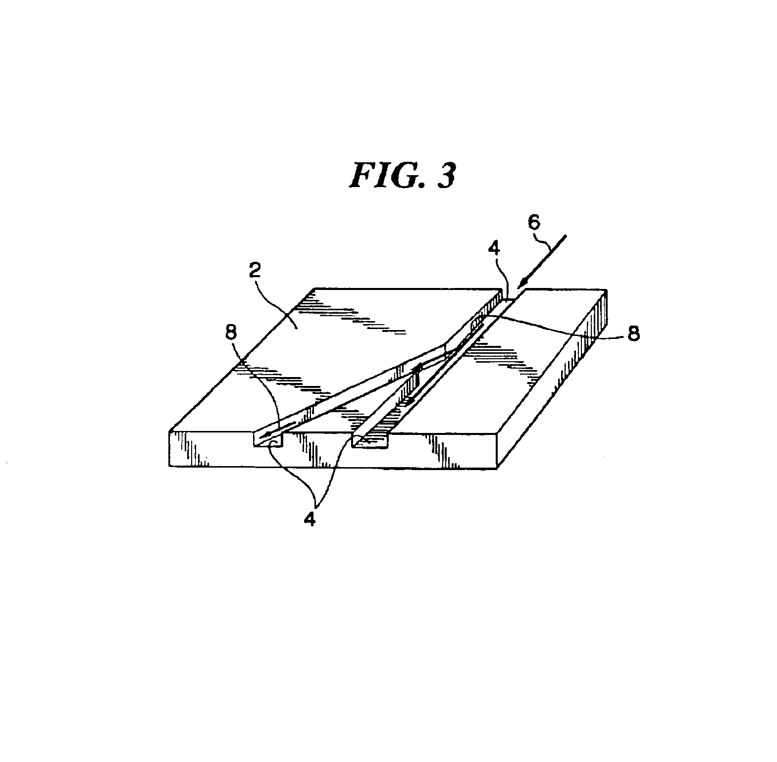
[0176]FIG. 11 is a schematic plan view showing the second embodiment of the carbon nanotube structure of the invention. On a surface of a given planar board 72, a carbon nanotube structure 78 made of carbon nanotubes 74 is fixed. In the embodiment, the carbon nanotube structure 78 in which the carbon nanotubes 74 are arranged along the desired patterning, is formed.

[0177]The carbon nanotube structure 78 of the embodiment can be manufactured as follows.

[0178]Using any of materials such as glass sheets and mica sheets, a hydrophobic surface is formed by applying the water-repellent treatment at the parts other than the patterning 76 on the surface of the planar board 72 to achieve the patterning 76 as shown in FIG. 11B. Then, only the patterning part 76 has hydrophobicity. Note that in the embodiment, using a silane coupling agent, the water-repellent treatment is applied.

[0179]Using the high-viscosity dispersing liquid W, in which a water-soluble medium is used for...

third embodiment

(Third Embodiment)

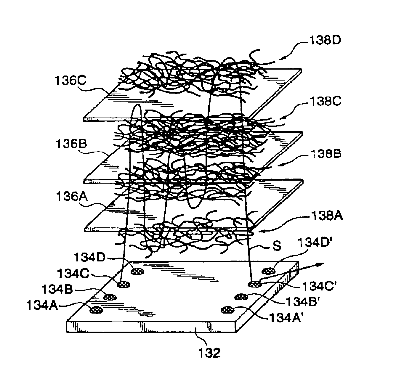
[0182]FIG. 12 is a schematic perspective view showing the third embodiment of the carbon nanotube structure of the invention. In the figure, convex parts 10 made of gold fine particles formed on the given planar board 12 are bound on the carbon nanotube structure 88 made of the carbon nanotubes 84.

[0183]In the third embodiment, first the convex parts 10 made of gold fine particles are formed on the planar board 12 as shown in FIG. 4A. Specifically, the convex parts 10 distributed like islands are formed by evaporating 20 nm of gold on the surface of the glass sheet, which is the planar board 12 and heating it. By spin-coating the high-viscosity dispersion medium to linked among and cover the whole gold fine particles like islands, the carbon nanotube structure 88 is formed.

[0184]In the embodiment, the convex parts 10 of gold fine particles like islands which are separated from each other, are electrically connected by the carbon nanotube structure 88.


PUM

PropertyMeasurementUnit
thicknessaaaaaaaaaa
diameteraaaaaaaaaa
emission currentaaaaaaaaaa

Abstract

Carbon nanotube structures are provided, in which the networks with a desired area and volume, where the carbon nanotubes are electrically or magnetically connected, are formed and the method for easily manufacturing the carbon nanotube structures with less carbon nanotube structures. Carbon nanotube devices are also provided, to which the useful carbon nanotube structures mentioned above are applied. A method for manufacturing carbon nanotube structures includes the steps of applying carbon nanotubes to a low-viscosity dispersion medium to obtain a high-viscosity dispersing liquid which includes carbon nanotubes, and forming a network of the carbon nanotubes having electrical and / or magnetic connections therebetween by removing the low-viscosity dispersion medium from the high-viscosity dispersed liquid.

Description

BACKGROUND OF THE INVENTION[0001]1. Field of the Invention[0002]This invention relates to a method for manufacturing carbon nanotube structures applicable to devices which contain carbon nanotubes, functional materials, and other structural materials, to the carbon nanotube structures, and to carbon nanotube devices using them.[0003]The invention can be extended to a wide variety of applications of carbon nanotubes.[0004]2. Description of the Related Art[0005]Fibrous carbons are generally called carbon fibers and conventionally, several kinds of methods for manufacturing carbon fibers having thickness of several μm or more in diameter used for structural materials have been studied. At present, among them, the method for manufacturing carbon fibers from PAN-based (polyacrylonitrile) and pitch-based materials is the most widely used.[0006]The method is briefly described as such a method, by which materials spun out from the PAN-based, isotropic pitch-based, and mesophase pitch-based ...

Claims


Application Information

Patent Timeline
Patent Type & Authority Patents(United States)
IPC IPC(8): C01B31/00C01B31/02D01F9/12B81B7/00B81C99/00B82B1/00B82B3/00H01L29/06
CPCB82Y15/00B82Y30/00B82Y40/00D01F9/12C01B31/0253Y10T428/2918Y10S977/742Y10S977/938C01B32/168
Inventor HORIUCHI, KAZUNAGASHIMIZU, MASAAKIYOSHIZAWA, HISAE
Owner FUJIFILM BUSINESS INNOVATION CORP
Why Eureka
Try Eureka