Gallium nitride-based light emitting diode and method of manufacturing the same

a technology of gallium nitride and light-emitting diodes, which is applied in the direction of semiconductor/solid-state device manufacturing, electrical equipment, semiconductors, etc., can solve the problems of degrading efficiency, cost-reducing or improving the optical power and chip characteristics, and difficulty in reducing the size of gans, etc., to achieve the effect of enhancing light extraction efficiency and maximizing the improvement effect of luminan

Active Publication Date: 2008-02-14
SAMSUNG ELECTRONICS CO LTD
View PDF7 Cites 62 Cited by
  • Summary
  • Abstract
  • Description
  • Claims
  • Application Information

AI Technical Summary

Benefits of technology

[0014] An advantage of the present invention is that it provides a vertical GaN-based LED in which an irregular-surface structure composed of an irregular-surface structure with even intervals and an irregular-surface structure with uneven intervals is formed on a light-emission portion of the vertical GaN-based LED. Therefore, light extraction efficiency is enhanced so that an improvement effect of luminance can be maximized.
[0015] Another advantage of the invention is that it provides a method of manufacturing the vertical GaN-based LED.
[0016] Additional aspect and advantages of the present general inventive concept will be set forth in part in the description which follows and, in part, will be obvious from the description, or may be learned by practice of the general inventive concept.
[0017] According to an aspect of the invention, a vertical GaN-based LED comprises an n-electrode; an n-type GaN layer formed under the n-electrode, the n-type GaN layer having an irregular-surface structure which includes a first irregular-surface structure having irregularities formed at even intervals and a second irregular-surface structure having irregularities formed at uneven intervals, the second irregular-surface structure being formed on the first irregular-surface structure; an active layer formed under the n-type GaN layer; a p-type GaN layer formed under the active layer; a p-electrode formed under the p-type GaN layer; and a structure support layer formed under the p-electrode.
[0018] According to another aspect of the invention, the vertical GaN-based LED further comprises a transparent conductive layer formed on the entire surface of the n-type GaN layer, the transparent conductive layer being positioned between the n-electrode and the n-type GaN layer.
[0019] According to a further aspect of the invention, a method of manufacturing a vertical GaN-based LED comprises sequentially forming an n-type GaN layer, an active layer, and a p-type GaN layer on a substrate; forming a p-electrode on the p-type GaN layer; forming a structure support layer on the p-electrode; removing the substrate so as to expose the surface of the n-type GaN layer; forming a first irregular-surface structure with even intervals on the exposed surface of the n-type GaN layer; forming a second irregular-surface structure with uneven intervals on the first irregular-surface structure; and forming an n-electrode on the n-type GaN layer having the first and second irregular-surface structures formed thereon.

Problems solved by technology

Therefore, it is difficult to reduce the size of the GaN-based LED for cost-down or improve the optical power and chip characteristics.
In general vertical GaN-based LEDs, however, efficiency where photons to be generated from an active layer are emitted to the outside is degraded.
Therefore, an improvement effect of luminance is not enough.

Method used


Image

  • Gallium nitride-based light emitting diode and method of manufacturing the same
  • Gallium nitride-based light emitting diode and method of manufacturing the same
  • Gallium nitride-based light emitting diode and method of manufacturing the same

Examples


first embodiment

[0050] First, a method of manufacturing a vertical GaN-based LED according to a first embodiment of the invention will be described in detail with reference to FIGS. 3 and 7A to 7E.

[0051]FIGS. 7A to 7E are sectional views sequentially showing the method of manufacturing a vertical GaN-based LED according to the first embodiment of the invention.

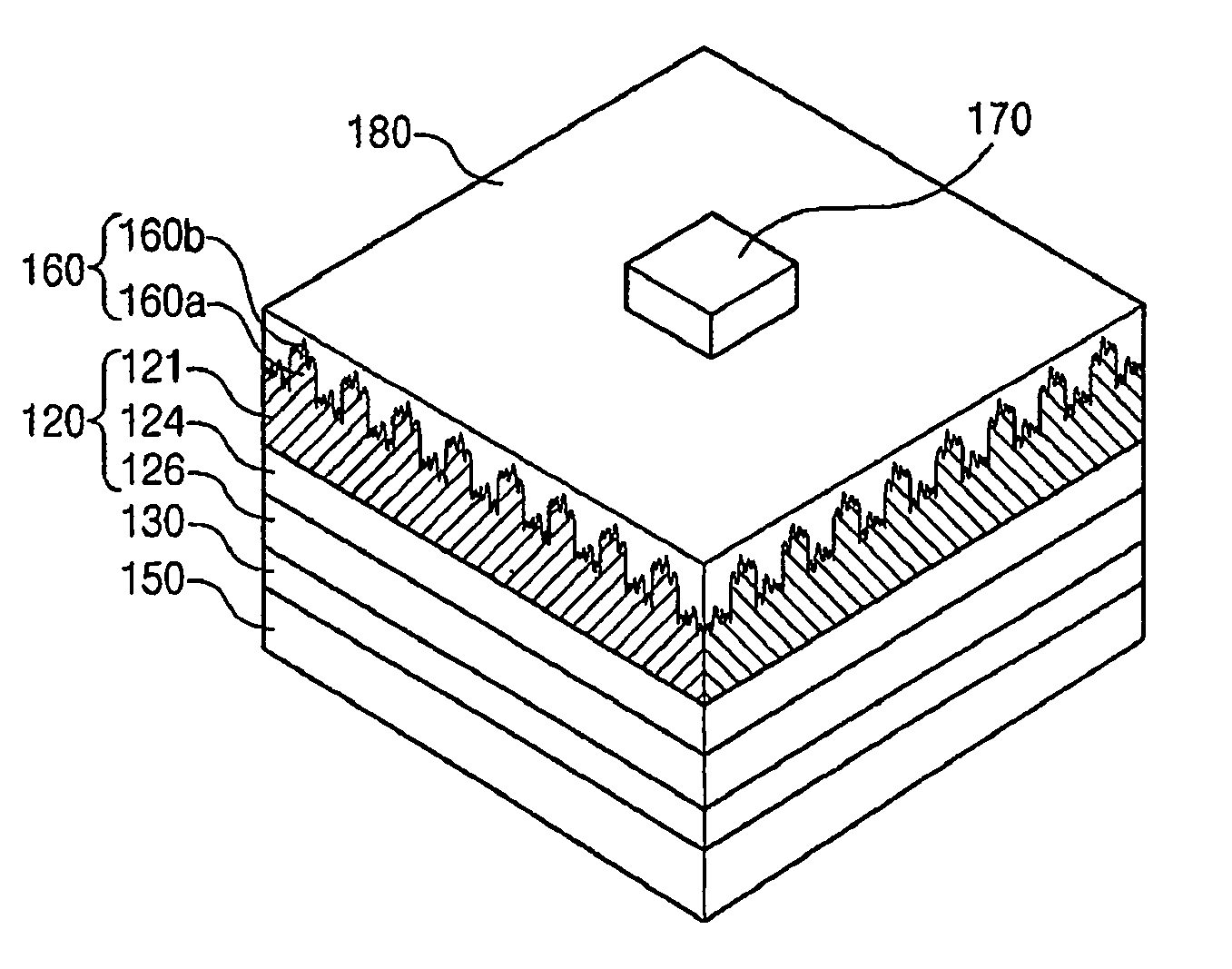
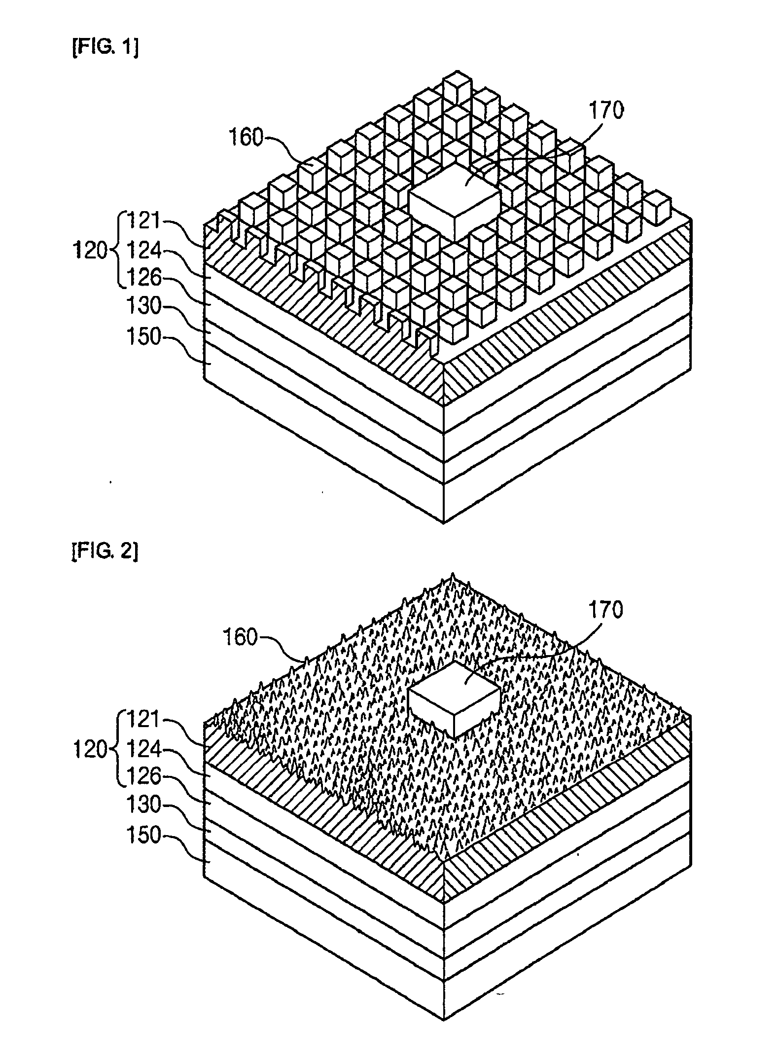
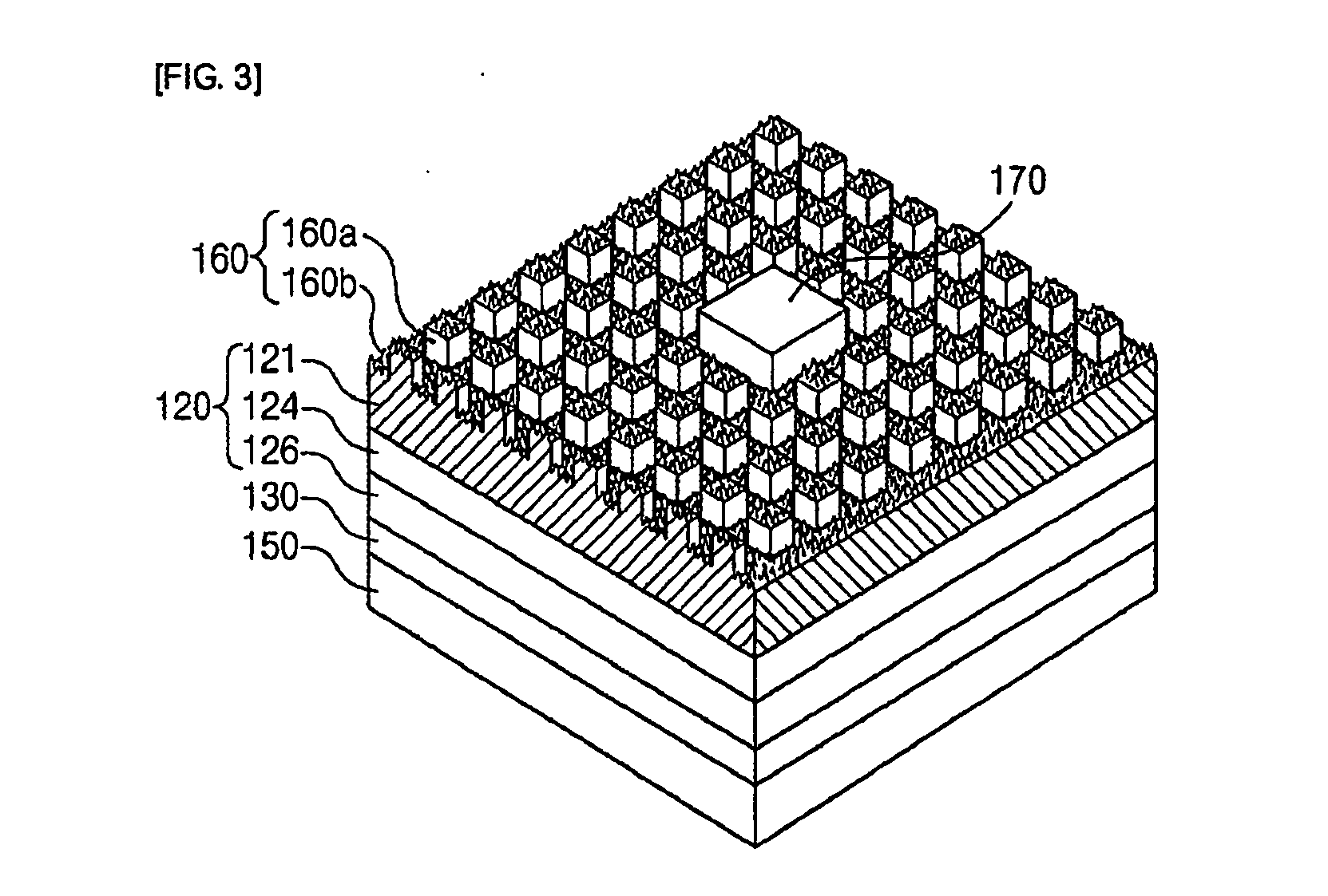
[0052] As shown in FIG. 7A, a light-emission structure 120 composed of a GaN-based semiconductor layer is formed on a substrate 100. In the light-emission structure 120, an n-type GaN layer 121, an active layer 124 formed of a GaN / InGaN layer having a multi-quantum well structure, and a p-type GaN layer 126 are sequentially laminated.

[0053] Preferably, the substrate 100 is formed of a transparent material including sapphire. In addition to sapphire, the substrate 100 may be formed of ZnO (zinc oxide), GaN (gallium nitride), SiC (silicon carbide), or AlN (aluminum nitride).

[0054] The n-type and p-type GaN-based semiconductor layer 121 and ...

second embodiment

[0066] Referring to FIGS. 3 and 8A to 8E, a method of manufacturing a vertical GaN-based LED according to a second embodiment of the invention will be described in detail.

[0067]FIGS. 8A to 8E are sectional views sequentially showing the method of manufacturing a vertical GaN-based LED according to the second embodiment of the invention.

[0068] As shown in FIG. 8A, first, a predetermined shape of photoresist pattern 200 with even intervals is formed on a substrate 100. Preferably, the substrate 100 is formed of a transparent material including sapphire. In addition to sapphire, the substrate 100 may be formed of ZnO (zinc oxide), GaN (gallium nitride), SiC (silicon carbide), or AlN (aluminum nitride).

[0069] Then, as shown in FIG. 8B, portions of the substrate 100 are selectively etched by using the photoresist pattern 200 as an etching mask such that an irregularity pattern 100a with even intervals is formed.

[0070] As shown in FIG. 8C, a GaN-based semiconductor layer is crystal-gr...


PUM


Abstract

A vertical GaN-based LED comprises an n-electrode; an n-type GaN layer formed under the n-electrode, the n-type GaN layer having an irregular-surface structure which includes a first irregular-surface structure having irregularities formed at even intervals and a second irregular-surface structure having irregularities formed at uneven intervals, the second irregular-surface structure being formed on the first irregular-surface structure; an active layer formed under the n-type GaN layer; a p-type GaN layer formed under the active layer; a p-electrode formed under the p-type GaN layer; and a structure support layer formed under the p-electrode.

Description

CROSS-REFERENCE TO RELATED APPLICATIONS [0001] This application claims the benefit of Korean Patent Application No. 10-2006-0076592 filed with the Korean Intellectual Property Office on Aug. 14, 2006, the disclosure of which is incorporated herein by reference. BACKGROUND OF THE INVENTION [0002] 1. Field of the Invention [0003] The present invention relates to a vertical gallium nitride-based light emitting diode (hereinafter, referred to as a vertical GaN-based LED) and a method of manufacturing the same, which can increases light extraction efficiency, thereby enhancing external quantum efficiency. [0004] 2. Description of the Related Art [0005] Generally, GaN-based LEDs are grown on a sapphire substrate. The sapphire substrate is a rigid nonconductor and has a low thermal conductivity. Therefore, it is difficult to reduce the size of the GaN-based LED for cost-down or improve the optical power and chip characteristics. Particularly, heat dissipation is very important for the LEDs...

Claims


Application Information

Patent Timeline
Patent Type & Authority Applications(United States)
IPC IPC(8): H01L33/00H01L21/20H01L33/06H01L33/22H01L33/32
CPCH01L33/22H01L33/02
Inventor BEOM, CHOI SEOKWON, OH BARIGGUN, WOO JONGGO, BAIK DOO
Owner SAMSUNG ELECTRONICS CO LTD
Why Eureka
Try Eureka