Light emitting element, light emitting device, manufacturing method of light emitting device, and sheet-like sealing material

a technology of light emitting elements and manufacturing methods, applied in the direction of discharge tubes/lamp details, organic semiconductor devices, discharge tubes luminescnet screens, etc., can solve the problem of limit on the improvement of power efficiency by the described method, and achieve the reduction of the total reflection of light which passes through the protective film, the reduction of the amount of total reflection of light, and the improvement of the light extraction efficiency of the light emitting element

Active Publication Date: 2008-01-24
SEMICON ENERGY LAB CO LTD
View PDF45 Cites 66 Cited by
  • Summary
  • Abstract
  • Description
  • Claims
  • Application Information

AI Technical Summary

Benefits of technology

[0020] In the above-described light emitting element of the present invention, the shape of the surface of the protective film is also changed by providing the fine particles having a predetermined refractive index onto the surface of the protective film on the light extraction side, similarly to the case of providing the fine particles onto the surface of the second electrode. Accordingly, the amount of total reflection of light which passes through the protective film is reduced, and light extraction efficiency of the light emitting element is improved.
[0021] When light emitted from a light emitting layer is extracted from a second electrode or a protective film, the amount of light which is totally reflected is reduced by the present invention. Accordingly, light extraction efficiency is improved. The improvement of the light extraction efficiency allows reduction of power consumption of a light emitting element and a light emitting device using the light emitting element. Particularly, the effect of the present invention to reduce the power consumption is more remarkably obtained by employing the top emission structure.

Problems solved by technology

However, there is a limitation on improvement in the power efficiency by the method described above.

Method used


Image

  • Light emitting element, light emitting device, manufacturing method of light emitting device, and sheet-like sealing material
  • Light emitting element, light emitting device, manufacturing method of light emitting device, and sheet-like sealing material
  • Light emitting element, light emitting device, manufacturing method of light emitting device, and sheet-like sealing material

Examples


embodiment mode 1

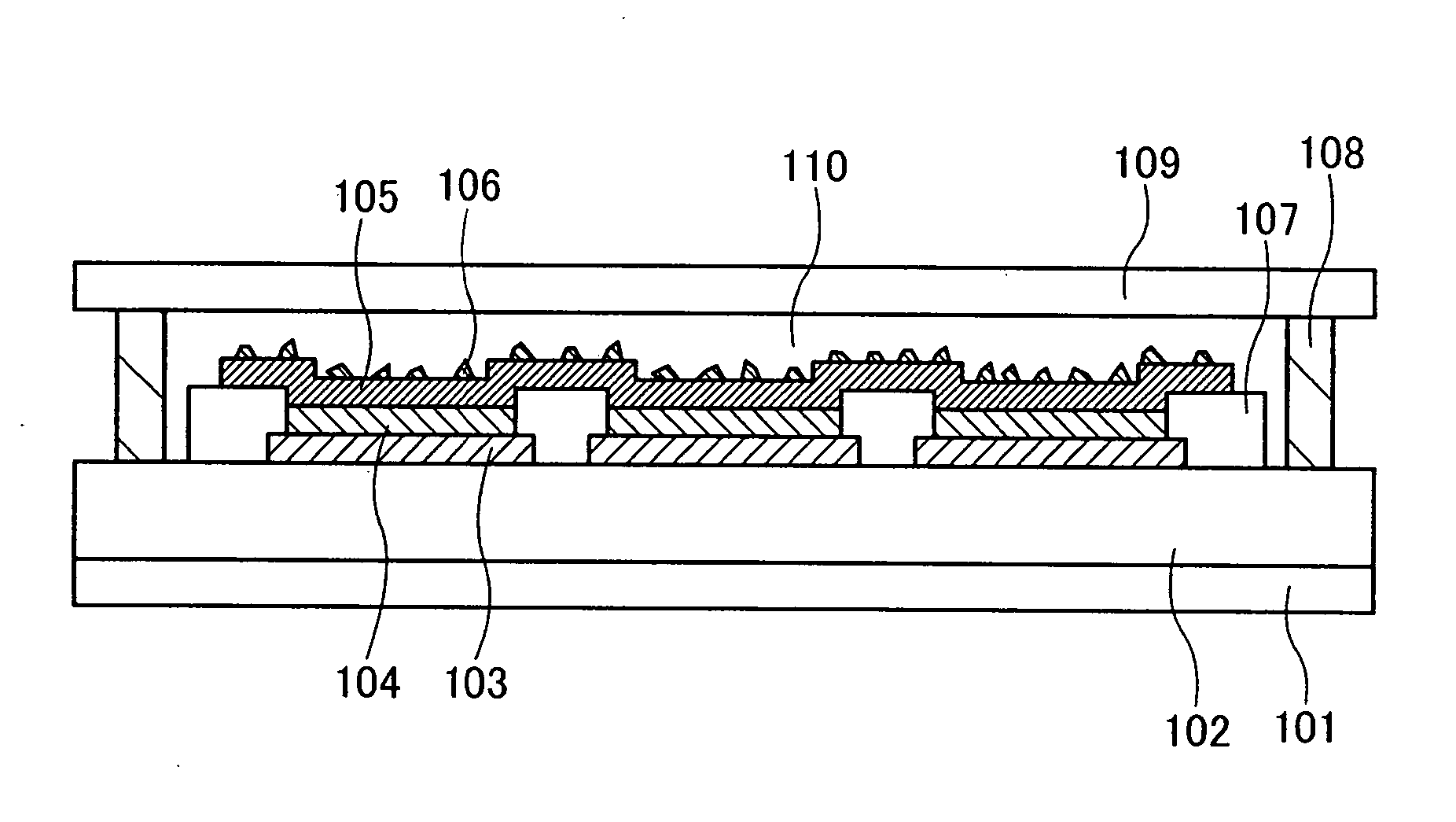
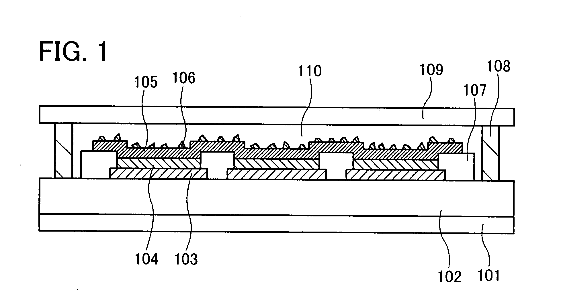
[0043]FIG. 1 is a cross sectional view of a light emitting device in which a light emitting element of this embodiment mode is provided. Over a substrate 101, a support 102 for a light emitting element is provided, and three light emitting elements are provided over the support 102.

[0044] In each light emitting element, a first electrode 103, a light emitting layer 104, and a second electrode 105 are sequentially stacked over the substrate 101. A plurality of fine particles 106 is provided on the second electrode 105, in contact with a surface of the second electrode 105. Note that the second electrode 105 is commonly provided for the three light emitting elements. An insulating layer 107 is provided for separating the light emitting elements each other, and is often called a partition wall.

[0045] A sealing substrate 109 is fixed to the substrate 101 with a sealing material 108 which is provided to surround a perimeter of the substrate 101, thereby sealing the light emitting eleme...

embodiment mode 2

[0075] Embodiment Mode 2 will be described with reference to FIGS. 2A to 2D. The air-sealed space between the substrate 101 and the substrate 109 is filled with a gas in Embodiment Mode 1. However, in a light emitting device of this embodiment mode, the space is filled with a solid material which is prepared by filling a liquid-phase material and curing it. A sealing structure of a light emitting device in which a solid is provided between substrates is called a solid sealing structure, and this word is frequently used to distinguish it from the structure in which a gas is filled. In this specification, this word will be used to distinguish the structure in which a solid is provided between substrates from the structure in which a gas is filled.

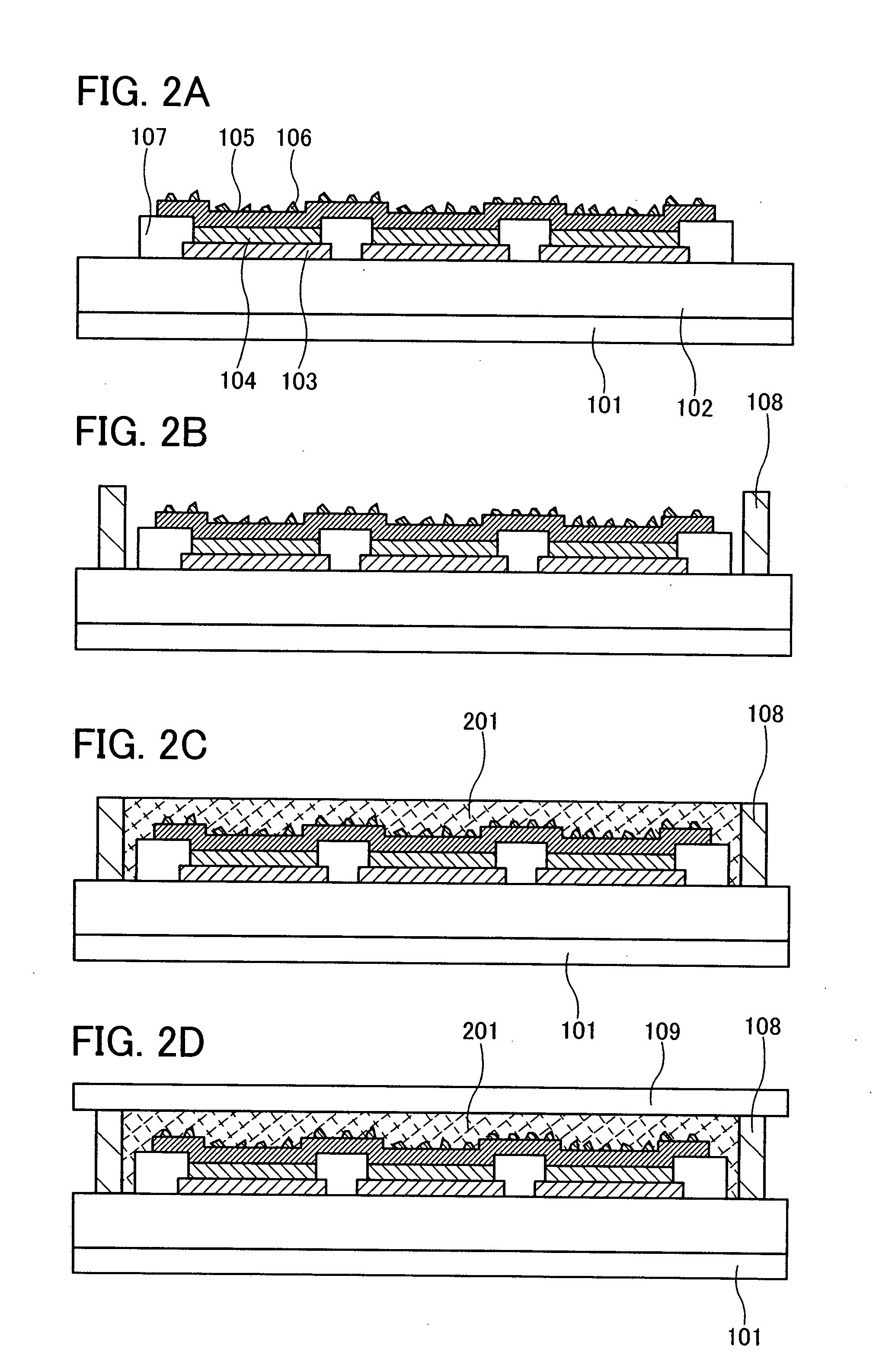
[0076] By applying the process described in Embodiment Mode 1, a substrate 101 over which fine particles 106 are sprayed on a surface of a second electrode 105 is prepared (FIG. 2A).

[0077] Next, an uncured sealing material 108 is provided w...

embodiment mode 3

[0080] Embodiment Mode 3 will be described with reference to FIGS. 3A to 3C. This embodiment mode will also describe a light emitting device having a solid sealing structure similar to Embodiment Mode 2.

[0081] By the process described in Embodiment Mode 1, a substrate 101 over which light emitting elements each including a first electrode 103, a light emitting layer 104, and a second electrode 105 are formed over a support 102 is prepared. In addition, before spraying fine particles, a sealing material 108 is provided on a perimeter of the substrate 101 as described in Embodiment Mode 1 (FIG. 3A).

[0082] An uncured (liquid-phase) filler 302 in which fine particles 106 are dispersed is prepared. As a material of the filler 302, similar materials to those of the filler 201 of Embodiment Mode 2 can be used. In a region surrounded by the sealing material 108, the uncured filler 302 in which the fine particles 106 are dispersed is dropwised (FIG. 3B).

[0083] The substrate 109 is provide...


PUM


Abstract

A method to improve light extraction efficiency of a light emitting element such as an electroluminescent element is disclosed. Over a substrate, a first electrode, a light emitting layer, and a second electrode are sequentially stacked. The first electrode is a reflective electrode. The second electrode is an electrode which transmits visible light, and light emitted from the light emitting layer is extracted from the second electrode. In contact with a surface of the second electrode, many fine particles are provided. The fine particles have a refractive index which is equal to or higher than that of the second electrode. Light which passes through the second electrode is scattered and refracted by the fine particles. Accordingly, the amount of light which is totally reflected at an interface between the second electrode and a gas is reduced, and light extraction efficiency is improved.

Description

BACKGROUND OF THE INVENTION [0001] 1. Field of the Invention [0002] The present invention relates to a light emitting element and a light emitting device including a light emitting element. In addition, the present invention relates to a method and a material for sealing a light emitting element. [0003] 2. Description of the Related Art [0004] Flat panel displays such as liquid crystal panels have been improved, and attempts have been made on improving quality of picture, reducing power consumption, and improving lifetime. In order to utilize the self-emitting ability of electroluminescent elements for practical application of electroluminescent panels (hereinafter referred to as an EL panels) which employs electroluminescent elements (hereinafter referred to as an EL elements) in the pixels, it is desired to realize vivid and bright displays with reduced power consumption. For this purpose, improvement in power efficiency has been investigated by increasing the current-luminance ch...

Claims


Application Information

Patent Timeline
Patent Type & Authority Applications(United States)
IPC IPC(8): H01L21/02
CPCH01L51/5246H01L51/5268H05B33/12H01L2251/5369H01L2251/5315H10K50/854H10K50/8426H10K2102/3026H10K2102/331H10K50/805H10K50/84
Inventor HIRAKATA, YOSHIHARU
Owner SEMICON ENERGY LAB CO LTD
Why Eureka
Try Eureka