Image processing device, image processing chip and image processing method

a technology of image processing device and image processing chip, which is applied in the direction of digital output to print units, input/output to record carriers, instruments, etc., can solve the problems of layout cost increase, inconvenience and disturbance for both manufacturers and users, and increase circuit complexities. , to achieve the effect of large circuit board size, large size and improved problem

Active Publication Date: 2016-06-21
MEDIATEK INC
View PDF5 Cites 0 Cited by
  • Summary
  • Abstract
  • Description
  • Claims
  • Application Information

AI Technical Summary

Benefits of technology

[0011]In the present invention, one single slot is provided on a circuit board or one single image receiving interface is provided on a chip to receive image signals in different image interface formats, thereby improving the issue caused by two slots or two image receiving interfaces in the prior art, such as a complex wiring layout on the circuit board, a large size of the circuit board and a large size resulted from a large pin count of the chip. Further, with a smaller number of slots, a signal receiving panel of a television or display device may be kept simple while providing better convenience.

Problems solved by technology

Therefore, to support various image interface formats, a circuit board in a television or display device is equipped with multiple slots, which increases not only circuit complexities but also layout costs.
The above shortcomings bring inconveniences and disturbances upon both manufacturers and users.

Method used


Image

  • Image processing device, image processing chip and image processing method
  • Image processing device, image processing chip and image processing method
  • Image processing device, image processing chip and image processing method

Examples


Embodiment Construction

[0017]Technical terms of the application are based on general definition in the technical field of the application. If the application describes or explains one or some terms, definition of the terms are based on the description or explanation of the application.

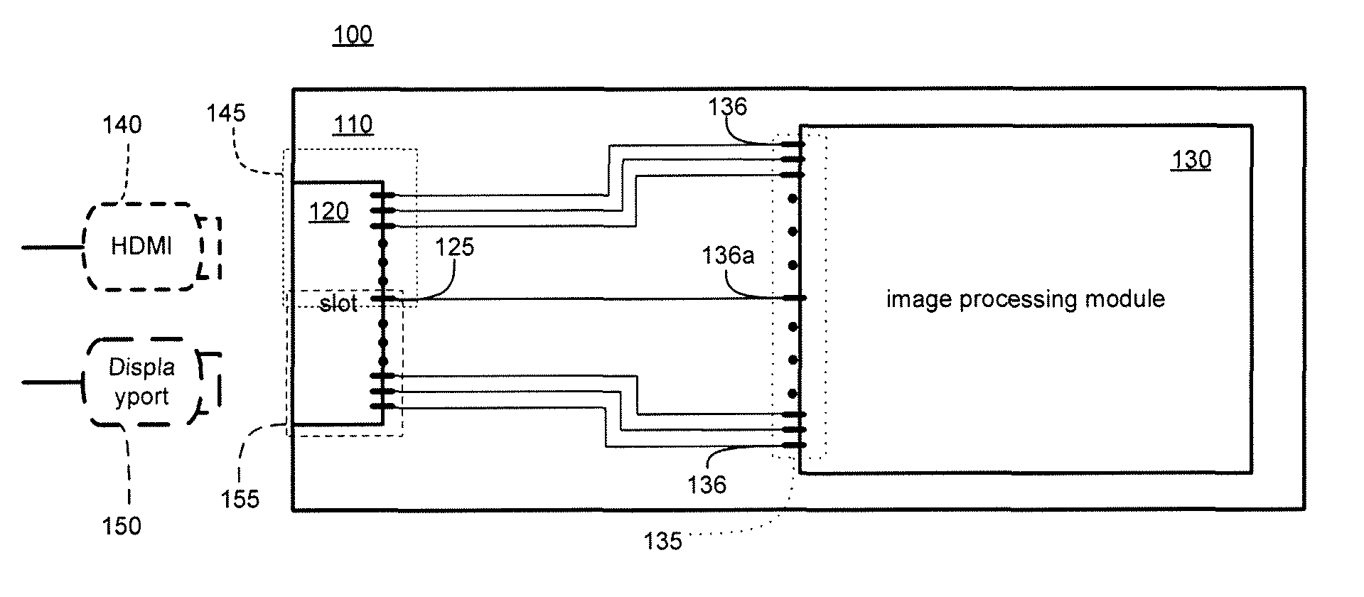
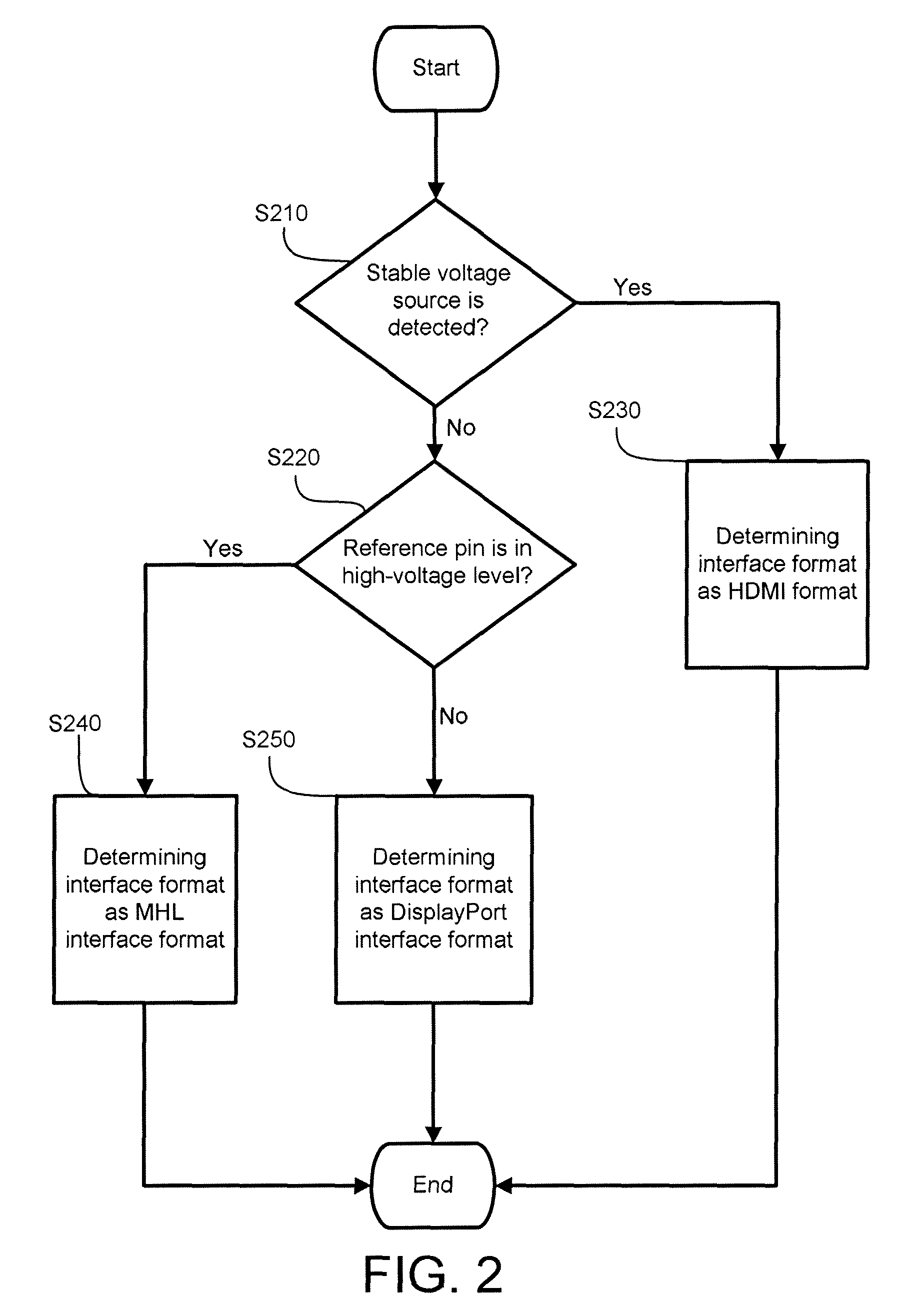
[0018]FIG. 1 shows a schematic diagram of an image processing device 100 according to an embodiment of the present invention. The image processing device 100 includes a circuit board 110, a slot 120 and an image processing module 130. The slot 120 is disposed on the circuit board 110, and is coupled to the image processing module 130. The slot 120 may be plugged in by both connectors 140 and 150 corresponding to different image interface formats. For example, the connector 140 may be a HDMI connector, and the connector 150 may be a DisplayPort interface connector. The image processing module 130 may be an image processing chip, e.g., an image scalar chip. Via a conducting wire between the slot 120 and the image processing mo...


PUM


Abstract

An image processing device for processing an image signal is provided. The image processing device includes a circuit board, a slot and an image processing module. The slot, disposed on the circuit board, is to be plugged in by either a first connector corresponding to a first image interface format or a second connector corresponding to a second image interface format. The image processing module, disposed on the circuit board and coupled to the slot, detects the image signal inputted from either the first connector or the second connector to determine a target image interface format, and processes the image signal by an image processing method corresponding to the target image interface format.

Description

[0001]This application claims the benefit of Taiwan application Serial No. 102128714, filed Aug. 9, 2013, the subject matter of which is incorporated herein by reference.BACKGROUND OF THE INVENTION[0002]1. Field of the Invention[0003]The invention relates in general to an image processing device, chip and method, and more particularly, to an image processing device, chip and method capable of automatically detecting and processing an image signal with a corresponding image processing method.[0004]2. Description of the Related Art[0005]Nowadays, most televisions and display devices support image signals in various image interface formats, e.g., High-Definition Multimedia Interface (HDMI) format, and DisplayPort interface format, and Mobile High-Definition Link (MHL) interface format. The HDMI connectors come in various types, of which a most common type A has 19 pins. The DisplayPort interface connectors have 20 pins. The MHL interface connector have two different ends—one end that c...

Claims


Application Information

Patent Timeline
Patent Type & Authority Patents(United States)
IPC IPC(8): G06F3/00H04N21/4402H04N21/4363G09G5/00G06F13/38G06F13/12G06F3/06G06F3/12
CPCG09G5/005H04N21/43635H04N21/4402G09G5/006G09G2370/10G09G2370/12G06F3/1206G06F3/0661
Inventor CHIANG, DIEN-SHENLIN, CHIN-LUNG
Owner MEDIATEK INC
Why Eureka
Try Eureka