Light emitting element
a technology of light-emitting elements and light-emitting components, which is applied in the direction of basic electric elements, electrical equipment, semiconductor devices, etc., can solve the problems of uneven brightness and uneven emission, and achieve the effect of reducing the number of light-emitting elements
- Summary
- Abstract
- Description
- Claims
- Application Information
AI Technical Summary
Problems solved by technology
Method used
Image

Examples
first embodiment
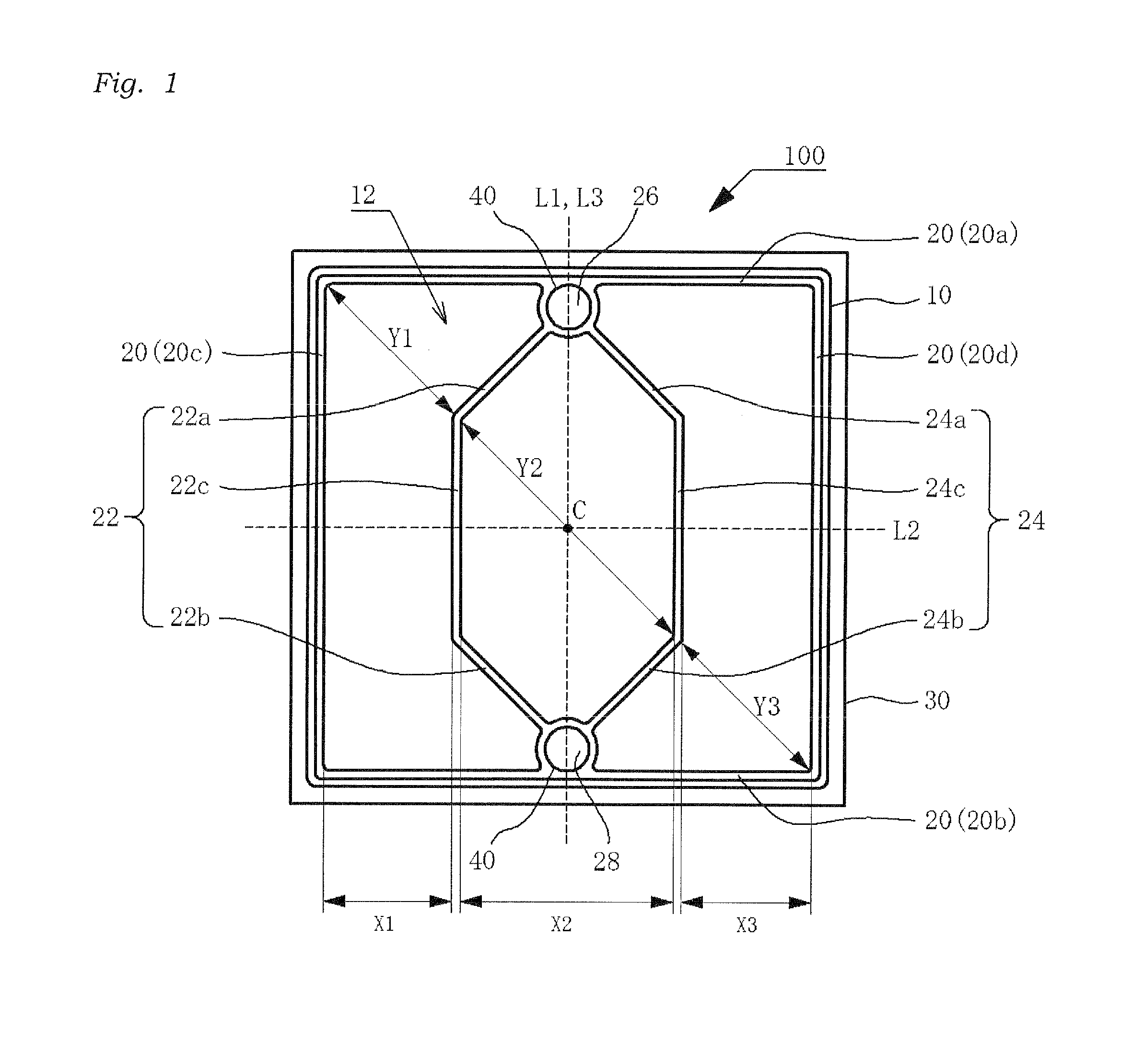
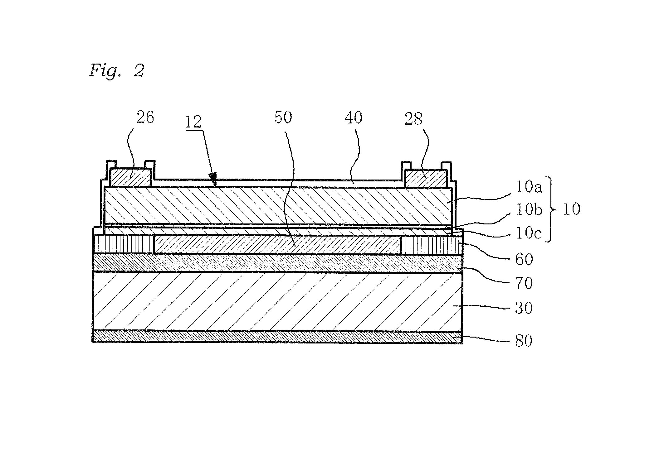
[0019]FIG. 1 is a schematic plan view, seen from an upper electrode side, of a light emitting element 100 according to a first embodiment. FIG. 2 is a schematic cross sectional view taken along line L1 of FIG. 1A, and FIG. 3 is a schematic cross sectional view taken along line L2 of FIG. 1. FIG. 4 is a diagram illustrating an emission intensity distribution of the light emitting element 100 according to the first embodiment, at an injection current of 500 mA.
[0020]As shown in FIGS. 1 to 4, the light emitting element 100 according to the first embodiment includes a semiconductor layer 10, an upper electrode disposed on an upper surface 12 of the semiconductor layer 10, and a lower electrode 50 disposed on a lower surface of the semiconductor layer 10, and has an approximately rectangular shape in a plan view. In a plan view, the upper electrode includes a first extending portion 20 extending in an approximately rectangular shape with four sides along an outer periphery of the semicon...
second embodiment
[0039]FIG. 5 is a schematic plan view, seen from an upper electrode side, of a light emitting element 200 according to a second embodiment. Next, the configurations different from those in the first embodiment will be described.
[0040]The light emitting element 200 according to the second embodiment differs from the light emitting element 100 in that the second extending portion 22 and the third extending portion 24 are arranged at opposite side of the first straight line L1 (in the region closer to the third side 20c and the region adjacent to the fourth side 20d of the first extending portion 20, respectively), each in a curved shape.
[0041]Accordingly, the area of the second extending portion 22 and the third extending portion 24 on the area of the upper surface 12 of the semiconductor layer 10 can be reduced and thus the light extraction efficiency can be enhanced. Further, bending portions can be eliminated from the second extending portion 22 and the third extending portion 24, ...
third embodiment
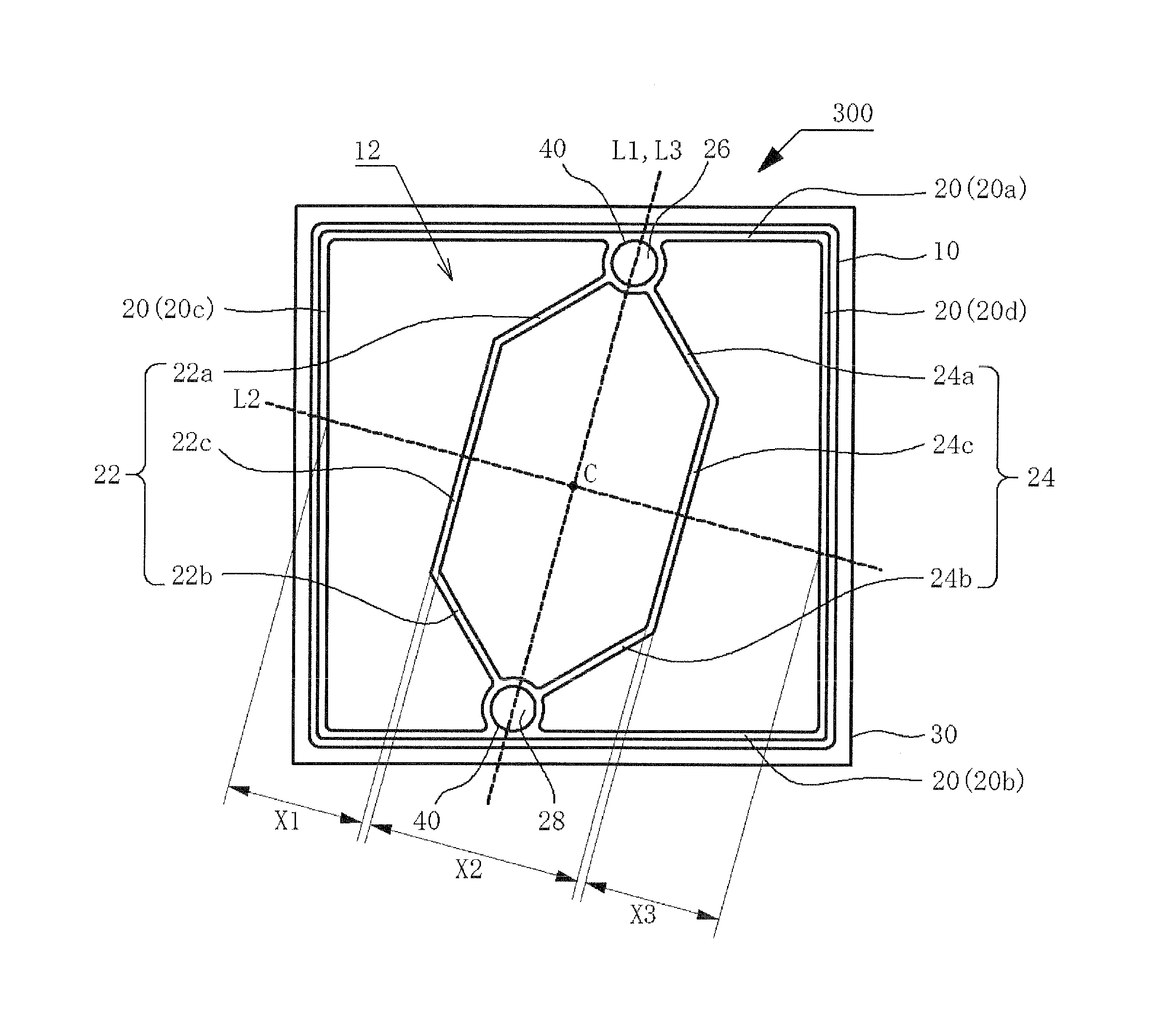
[0042]FIG. 6 is a schematic plan view, seen from an upper electrode side, of a light emitting element according to a third embodiment. Next, a light emitting device according to the second embodiment will be described.
[0043]The light emitting element 300 according to the third embodiment differs from the light emitting element 100 in that the first straight line L1 connecting the first pad portion 26 and the second pad portion 28 in a shortest distance is arranged passing through the intersection point of the diagonal lines of the first extending portion 20 and at an angle to the third side 20c and the fourth side 20d which are among the four sides of the first extending portion 20 and are not provided with the pad portion 26 or 28. The second extending portion 22 and the third extending portion 24 each connecting the pad portions 26 and 28 are arranged symmetrically with respect to the inclined first straight line L1.
[0044]This configuration allows for a longer distance between the...
PUM
 Abstract
Description
Claims
Application Information
 - R&D
- Intellectual Property
- Life Sciences
- Materials
- Tech Scout
- Unparalleled Data Quality
- Higher Quality Content
- 60% Fewer Hallucinations
Browse by: Latest US Patents, China's latest patents, Technical Efficacy Thesaurus, Application Domain, Technology Topic, Popular Technical Reports.
© 2025 PatSnap. All rights reserved.Legal|Privacy policy|Modern Slavery Act Transparency Statement|Sitemap|About US| Contact US: help@patsnap.com