
Superjunction device and method of manufacturing the same
A manufacturing method and super junction technology, which is applied in semiconductor/solid-state device manufacturing, semiconductor devices, electrical components, etc., can solve the problems of complex implantation process, sharp reverse recovery fluctuation, and increased process cost, etc.
Patent Information
- Authority / Receiving Office
- CN · China
- Patent Type
- Patents(China)
- Current Assignee / Owner
- Publication Date
- 2017-03-29
Smart Images
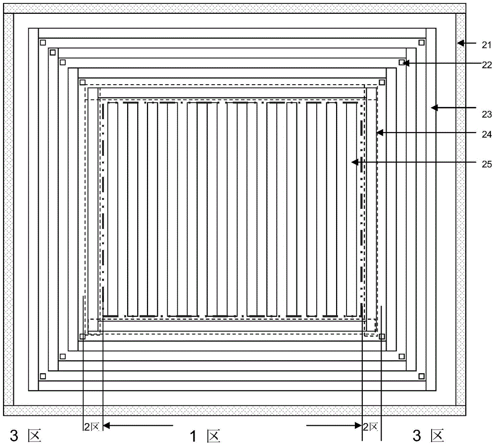
Figure 1 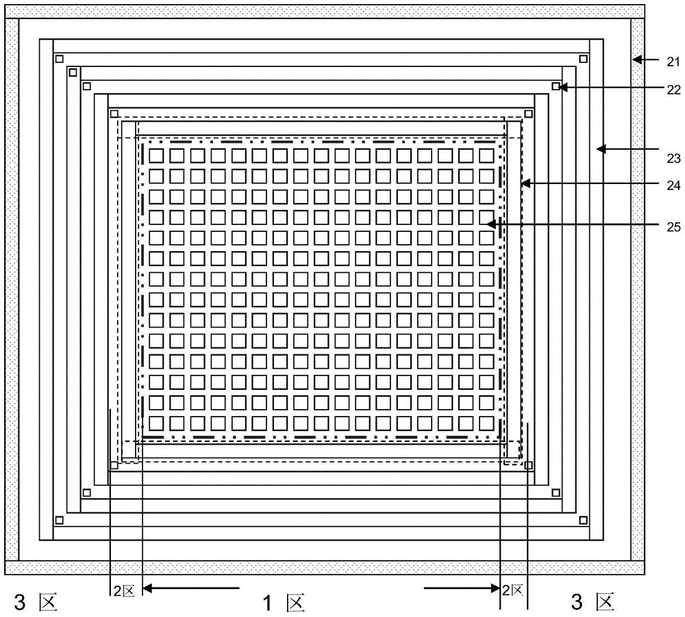
Figure 2 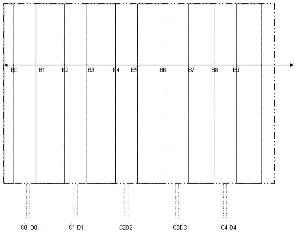
Figure 3
Abstract
Description
Technical field
[0001] The invention relates to the field of semiconductor integrated circuit manufacturing, in particular to a super junction device; the invention also relates to a manufacturing method of a super junction device. Background technique
[0002] Super junction MOSFET adopts a new withstand voltage layer structure, using a series of alternately arranged P-type semiconductor thin layers and N-type semiconductor thin layers to combine the P-type semiconductor thin layers and N-type semiconductor thin layers at a lower voltage in the off state. Type semiconductor thin layer is depleted to achieve mutual compensation of charges, so that P-type semiconductor thin layer and N-type semiconductor thin layer can achieve high breakdown voltage under high doping concentration, thereby achieving low on-resistance and high breakdown at the same time Voltage, breaking the theoretical limit of traditional power MOSFET. In the US patent US5216275, the above alternately arranged P...
Examples
Embodiment Construction
[0120] Such as figure 1 Shown is the top view of the existing super junction device Figure one . In the top view, the embodiment of the present invention can be divided into zone 1, zone 2, and zone 3. Region 1 is the middle region of the super junction device, which is the current flow region. The current flow region includes alternately arranged P-type regions 25 and N-type regions. The P-type region 25 is also the P-type region formed in the current flow region. The N-type thin layer, the N-type region is also the N-type thin layer formed in the current flow region; in the current flow region, the current will pass through the N-type region from the source to the drain through the channel, and the The P-type region 25 and the N-type region form a depletion region to withstand voltage in the reverse blocking state. Zone 2 and Zone 3 are the terminal protection structure area of the super junction device. When the device is turned on, the terminal protection structure does...